Hostname: page-component-cd9895bd7-gbm5v Total loading time: 0 Render date: 2025-01-04T00:35:06.255Z Has data issue: false hasContentIssue false

Effect of underlying boron nitride thickness on photocurrent response in molybdenum disulfide - boron nitride heterostructures

Published online by Cambridge University Press:  06 January 2016

Milinda Wasala
Affiliation:
Department of Physics, Southern Illinois University Carbondale, Carbondale, Illinois 62901, USA
Jie Zhang
Affiliation:
Department of Physics, Southern Illinois University Carbondale, Carbondale, Illinois 62901, USA
Sujoy Ghosh
Affiliation:
Department of Physics, Southern Illinois University Carbondale, Carbondale, Illinois 62901, USA
Baleeswaraiah Muchharla
Affiliation:
Department of Physics, Southern Illinois University Carbondale, Carbondale, Illinois 62901, USA
Rachel Malecek
Affiliation:
Department of Physics, Southern Illinois University Carbondale, Carbondale, Illinois 62901, USA
Dipanjan Mazumdar
Affiliation:
Department of Physics, Southern Illinois University Carbondale, Carbondale, Illinois 62901, USA
Hassana Samassekou
Affiliation:
Department of Physics, Southern Illinois University Carbondale, Carbondale, Illinois 62901, USA
Moses Gaither-Ganim
Affiliation:
Department of Physics, Southern Illinois University Carbondale, Carbondale, Illinois 62901, USA
Andrew Morrison
Affiliation:
Department of Physics, Southern Illinois University Carbondale, Carbondale, Illinois 62901, USA
Nestor-Perera Lopez
Affiliation:
Department of Physics and Center for 2-Dimensional and Layered Materials, The Pennsylvania State University, University Park, Pennsylvania 16802, USA
Victor Carozo
Affiliation:
Department of Physics and Center for 2-Dimensional and Layered Materials, The Pennsylvania State University, University Park, Pennsylvania 16802, USA
Zhong Lin
Affiliation:
Department of Physics and Center for 2-Dimensional and Layered Materials, The Pennsylvania State University, University Park, Pennsylvania 16802, USA
Mauricio Terrones
Affiliation:
Department of Physics and Center for 2-Dimensional and Layered Materials, The Pennsylvania State University, University Park, Pennsylvania 16802, USA; and Department of Chemistry and Department of Materials Science and Engineering, The Pennsylvania State University, University Park, Pennsylvania 16802, USA
Saikat Talapatra*
Affiliation:
Department of Physics, Southern Illinois University Carbondale, Carbondale, Illinois 62901, USA
*
a) Address all correspondence to this author. e-mail: stalapatra@physics.siu.edu
Get access

Abstract

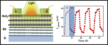
Here we report on the photocurrent response of two-dimensional (2D) heterostructures of sputtered MoS2 on boron nitride (BN) deposited on (001)-oriented Si substrates. The steady state photocurrent (I ph) measurements used a continuous laser of λ = 658 nm (E = 1.88 eV) over a broad range of laser intensities, P (∼1 μW < P < 10 μW), and indicate that I ph obtained from MoS2 layers with the 80 nm BN under layer was ∼4 times higher than that obtained from MoS2 layers with the 30 nm BN under layer. We also found super linear dependence of I ph on P (I phP γ, with γ > 1) in both the samples. The responsivities obtained over the range of laser intensity studied were in the order of mA/W (∼12 and ∼2.7 mA/W with 80 nm BN and 30 nm BN under layers, respectively). These investigations provide crucial insight into the optical activity of MoS2 on BN, which could be useful for developing a variety of optoelectronic applications with MoS2 or other 2D transition metal dichalcogenide heterostructures.

Type
Invited Articles
Copyright
Copyright © Materials Research Society 2016 

Access options

Get access to the full version of this content by using one of the access options below. (Log in options will check for institutional or personal access. Content may require purchase if you do not have access.)

References

REFERENCES

Novoselov, K.S., Jiang, D., Schedin, F., Booth, T.J., Khotkevich, V.V., Morozov, S.V., and Geim, A.K.: Two-dimensional atomic crystals. Proc. Natl. Acad. Sci. U. S. A. 102, 10451 (2005).CrossRefGoogle ScholarPubMed
Jariwala, D., Sangwan, V.K., Lauhon, L.J., Marks, T.J., and Hersam, M.C.: Emerging device applications for semiconducting two-dimensional transition metal dichalcogenides. ACS Nano 8, 1102 (2014).Google Scholar
Pradhan, N., Rhodes, D.A., Memaran, S., Poumirol, J.M., Smirnov, D., Talapatra, S., Feng, S., Perea-López, N., Elias, A.L., Terrones, M., Ajayan, P.M., and Balicas, L.: Hall and field-effect mobilities in few layered p-WSe2 field-effect transistors. Sci. Rep. 5, 8979 (2015).CrossRefGoogle ScholarPubMed
Radisavljevic, B., Radenovic, A., Brivio, J., Giacometti, V., and Kis, A.: Single-layer MoS2 transistors. Nat. Nanotechnol. 6, 147 (2011).CrossRefGoogle ScholarPubMed
Ghosh, S., Najmaei, S., Kar, S., Vajtai, R., Pradhan, N., Lou, J., Balicas, L., Ajayan, P.M., and Talapatra, S.: Universal ac conductance in large area CVD grown MoS2 . Phys. Rev. B 89, 125422 (2014).Google Scholar
Wang, Q.H., Kalantar-Zadeh, K., Kis, A., Coleman, J.N., and Strano, M.S.: Electronics and optoelectronics of two-dimensional transition metal dichalcogenides. Nat. Nanotechnol. 7, 699 (2012).Google Scholar
Kim, S., Konar, A., Hwang, W., Lee, J.H., Lee, J., Yang, J., Jung, C., Kim, H., Yoo, J.B., Choi, J.Y., Jin, Y.W., Lee, S.Y., Jena, D., Choi, W., and Kim, K.: High-mobility and low-power thin-film transistors based on multilayer MoS2 crystals. Nat. Commun. 3, 1011 (2012).Google Scholar
Zhang, Y., Ye, J., Matsuhashi, Y., and Iwasa, Y.: Ambipolar MoS2 thin flake transistors. Nano Lett. 12, 1136 (2012).Google Scholar
Yin, Z., Li, H., Li, H., Jiang, L., Shi, Y., Sun, Y., Lu, G., Zhang, Q., Chen, X., and Zhang, H.: Single-layer MoS2 phototransistors. ACS Nano 6(1), 74 (2012).CrossRefGoogle ScholarPubMed
Lee, H.S., Min, S.W., Chang, Y.G., Park, M.K., Nam, T., Kim, H., Kim, J.H., Ryu, S., and Im, S.: MoS2 nanosheet phototransistors with thickness-modulated optical energy gap. Nano Lett. 12(7), 3695 (2012).CrossRefGoogle ScholarPubMed
Ghosh, S., Winchester, A., Muchharla, B., Wasala, M., Feng, S., Elias, A.L., Krishna, M.B.M., Harada, T., Chin, C., Dani, K., Kar, S., Terrones, M., and Talapatra, S.: Ultrafast intrinsic photoresponse and direct evidence of sub-gap states in liquid phase exfoliated MoS2 thin films. Sci. Rep. 5, 11272 (2015).Google Scholar
Bao, W., Cai, X., Kim, D., Sridhara, K., and Fuhrer, M.S.: High mobility ambipolar MoS2 field-effect transistors: Substrate and dielectric effects. Appl. Phys. Lett. 102, 042104 (2013).Google Scholar
Bilgin, I., Liu, F., Vargas, A., Winchester, A., Man, M.K.L., Upmanyu, M., Dani, K., Gupta, G., Talapatra, S., Mohite, A.D., and Kar, S.: Chemical vapor deposition synthesized atomically-thin molybdenum disulfide with optoelectronic-grade crystalline quality. ACS Nano 9(9), 8822 (2015).Google Scholar
Buscema, M., Steele, G.A., van der Zant, H.S.J., and Castellanos-Gomez, A.: The effect of the substrate on the Raman and photoluminescence emission of single-layer MoS2 . Nano Res. 7, 561 (2014).Google Scholar
Lien, D-H., Kang, J.S., Amani, M., Chen, K., Tosun, M., Wang, H-P., Roy, T., Eggleston, M.S., Wu, M.C., Dubey, M., Lee, S-C., He, J-H., and Javey, A.: Engineering light outcoupling in 2D materials. Nano Lett. 15, 1356 (2015).Google Scholar
Gong, Y., Lin, J., Wang, X., Shi, G., Lei, S., Lin, Z., Zou, X., Ye, G., Vajtai, R., Yakobson, B.I., Terrones, H., Terrones, M., Tay, B.K., Lou, J., Pantelides, S.T., Liu, Z., Zhou, W., and Ajayan, P.M.: Vertical and in-plane heterostructures from WS2/MoS2 monolayers. Nat. Mater. 13, 1135 (2014).Google Scholar
Liu, Z., Song, L., Zhao, S., Huang, J., Ma, L., Zhang, J., Lou, J., and Ajayan, P.M.: Direct growth of graphene/hexagonal boron nitride stacked layers. Nano Lett. 11(5), 2032 (2011).Google Scholar
Shi, Y., Zhou, W., Lu, A.Y., Fang, W., Lee, Y.H., Hsu, A.L., Kim, S.M., Kim, K.K., Yang, H.Y., Li, L.J., Idrobo, J.C., and Kong, J.: van der Waals epitaxy of MoS2 layers using graphene as growth templates. Nano Lett. 12(6), 2784 (2012).CrossRefGoogle Scholar
Okada, M., Sawazaki, T., Watanabe, K., Taniguch, T., Hibino, H., Shinohara, H., and Kitaura, R.: Direct chemical vapor deposition growth of WS2 atomic layers on hexagonal boron nitride. ACS Nano 8(8), 8273 (2014).Google Scholar
Zhang, X., Meng, F., Christianson, J.R., Arroyo-Torres, C., Lukowski, M.A., Liang, D., Schmidt, J.R., and Jin, S.: Vertical heterostructures of layered metal chalcogenides by van der Waals epitaxy. Nano Lett. 14(6), 3047 (2014).Google Scholar
Björck, M. and Andersson, G.: GenX: An extensible x-ray reflectivity refinement program utilizing differential evolution. J. Appl. Cryst. 40, 1174 (2007).Google Scholar
Windom, B.C., Sawyer, W.G., and Hahn, D.W.: A Raman spectroscopic study of MoS2 and MoO3: Applications to tribological systems. Tribol. Lett. 42(3), 301 (2011).Google Scholar
Li, H., Zhang, Q., Yap, C.C.R., Tay, B.K., Edwin, T.H.T., Olivier, A., and Baillargeat, D.: From bulk to monolayer MoS2: Evolution of Raman scattering. Adv. Funct. Mater. 22, 1385 (2012).Google Scholar
Lee, C., Yan, H., Brus, L.E., Heinz, T.F., Hone, J., and Ryu, S.: Anomalous lattice vibrations of single- and few-layer MoS2 . ACS Nano 4(5), 2695 (2010).Google Scholar
Boukhicha, M., Calandra, M., Measson, M.A., Lancry, O., and Shukla, A.: Anharmonic phonons in few-layer MoS2: Raman spectroscopy of ultralow energy compression and shear modes. Phys. Rev. B 87, 195316 (2013).CrossRefGoogle Scholar
Rose, A.: Recombination processes in insulators and semiconductors. Phys. Rev. 97(2), 322 (1955).CrossRefGoogle Scholar
Perea-López, N., Elías, A.L., Berkdemir, A., Castro-Beltran, A., Gutiérrez, H.R., Feng, S., Lv, R., Hayashi, T., López-Urías, F., Ghosh, S., Muchharla, B., Talapatra, S., Terrones, H., and Terrones, M.: Photosensor device based on few-layered WS2 films. Adv. Funct. Mater. 23, 5511 (2013).Google Scholar
Kundu, S., Ghosh, S., Fralaide, M., Narayanan, T.N., Pillai, V.K., and Talapatra, S.: Fractional photo-current dependence of graphene quantum dots prepared from carbon nanotubes. Phys. Chem. Chem. Phys. 17, 24566 (2015).Google Scholar
Chi, K.K.: Dielectric Phenomena in Solids (Academic Press, Burlington, 2004).Google Scholar
Mott, N.F. and Davis, E.: Electronic Processes in Non-crystalline Materials (Oxford University Press, London, 1971).Google Scholar
Kushwaha, N., Kushwaha, V.S., Shukla, R.K., and Kumar, A.: Determination of energy of defect centers in a-Se78Ge22 thin films. Philos. Mag. Lett. 86, 691 (2006).CrossRefGoogle Scholar
Bakr, N.A.: Anomalous photoconductive transport properties of As2Se3 films. Egypt. J. Sol. 25, 13 (2002).Google Scholar
Klee, V., Preciado, E., Barroso, D., Nguyen, A.E., Lee, C., Erickson, K.J., Triplett, M., Davis, B., Lu, I-H., Bobek, S., McKinley, J., Martinez, J.P., Mann, J., Talin, A.A., Bartels, L., and Léonard, F.: Superlinear composition-dependent photocurrent in CVD-grown monolayer MoS2(1–x)Se2x alloy devices. Nano Lett. 15, 2612 (2015).CrossRefGoogle ScholarPubMed
Qiu, H., Pan, L., Yao, Z., Li, J., Shi, Y., and Wang, X.: Electrical characterization of back-gated bi-layer MoS2 field-effect transistors and the effect of ambient on their performances. Appl. Phys. Lett. 100, 123104 (2012).Google Scholar
Park, W., Park, J., Jang, J., Lee, H., Jeong, H., Cho, K., Hong, S., and Lee, T.: Oxygen environmental and passivation effects on molybdenum disulfide field effect transistors. Nanotechnology 24, 095202 (2013).Google Scholar