Crossref Citations
This article has been cited by the following publications. This list is generated based on data provided by
Crossref.
Molaei, R.
Bayati, R.
Nori, S.
Kumar, D.
Prater, J. T.
and
Narayan, J.
2013.
Diamagnetic to ferromagnetic switching in VO2 epitaxial thin films by nanosecond excimer laser treatment.
Applied Physics Letters,
Vol. 103,
Issue. 25,
Molaei, R.
Bayati, M. R.
Alipour, H. M.
Nori, S.
and
Narayan, J.
2013.
Enhanced photocatalytic efficiency in zirconia buffered n-NiO/p-NiO single crystalline heterostructures by nanosecond laser treatment.
Journal of Applied Physics,
Vol. 113,
Issue. 23,
Jian, Jie
Chen, Aiping
Zhang, Wenrui
and
Wang, Haiyan
2013.
Sharp semiconductor-to-metal transition of VO2 thin films on glass substrates.
Journal of Applied Physics,
Vol. 114,
Issue. 24,
Molaei, R.
Bayati, R.
Wu, F.
and
Narayan, J.
2014.
A microstructural approach toward the effect of thickness on semiconductor-to-metal transition characteristics of VO2 epilayers.
Journal of Applied Physics,
Vol. 115,
Issue. 16,
Bayati, Reza
Molaei, Roya
Wu, Fan
Narayan, Jagdish
Yarmolenko, Sergey
and
Paranthaman, P.
2015.
Dependence of Semiconductor to Metal Transition of VO2(011)/NiO{100}/MgO{100}/TiN{100}/Si{100} Heterostructures on Thin Film Epitaxy and Nature of Strain.
Journal of the American Ceramic Society,
Vol. 98,
Issue. 4,
p.
1201.
Montero, José
Ji, Yu-Xia
Li, Shu-Yi
Niklasson, Gunnar A.
and
Granqvist, Claes G.
2015.
Sputter deposition of thermochromic VO2 films on In2O3:Sn, SnO2, and glass: Structure and composition versus oxygen partial pressure.
Journal of Vacuum Science & Technology B, Nanotechnology and Microelectronics: Materials, Processing, Measurement, and Phenomena,
Vol. 33,
Issue. 3,
Miyazaki, Kenichi
Shibuya, Keisuke
Suzuki, Megumi
Wado, Hiroyuki
and
Sawa, Akihito
2015.
High temperature coefficient of resistance of low-temperature-grown VO2 films on TiO2-buffered SiO2/Si (100) substrates.
Journal of Applied Physics,
Vol. 118,
Issue. 5,
Singamaneni, Srinivasa Rao
Prater, John Thomas
and
Narayan, Jagdish
2016.
Multifunctional epitaxial systems on silicon substrates.
Applied Physics Reviews,
Vol. 3,
Issue. 3,
p.
031301.
Choi, Songhee
Chang, Sung‐Jin
Oh, Junhyeob
Jang, Jae Hyuck
and
Lee, Shinbuhm
2018.
Electrical and Optical Properties of VO2 Polymorphic Films Grown Epitaxially on Y‐Stabilized ZrO2.
Advanced Electronic Materials,
Vol. 4,
Issue. 6,
Choi, Songhee
Son, Jaeseok
Oh, Junhyeob
Lee, Ji-Hyun
Jang, Jae Hyuck
and
Lee, Shinbuhm
2019.
Sharp contrast in the electrical and optical properties of vanadium Wadsley
(VmO2m+1,m>1)
epitaxial films selectively stabilized on (111)-oriented Y-stabilized
ZrO2.
Physical Review Materials,
Vol. 3,
Issue. 6,
Moatti, Adele
Sachan, Ritesh
Cooper, Valentino R
and
Narayan, Jagdish
2019.
Electrical Transition in Isostructural VO2 Thin-Film Heterostructures.
Scientific Reports,
Vol. 9,
Issue. 1,
Vu, Tuan Duc
Chen, Zhang
Zeng, Xianting
Jiang, Meng
Liu, Shiyu
Gao, Yanfeng
and
Long, Yi
2019.
Physical vapour deposition of vanadium dioxide for thermochromic smart window applications.
Journal of Materials Chemistry C,
Vol. 7,
Issue. 8,
p.
2121.
Choi, Songhee
Oh, Junhyeob
Lee, Ji-Hyun
Jang, Jae Hyuck
and
Lee, Shinbuhm
2019.
Degradation Mechanism of Vanadium Oxide Films When Grown on Y‐Stabilized ZrO2 Above 500 °C.
Advanced Engineering Materials,
Vol. 21,
Issue. 12,
Le, Phu Tran Phong
Hofhuis, Kevin
Rana, Abhimanyu
Huijben, Mark
Hilgenkamp, Hans
Rijnders, Guus A.J.H.M.
ten Elshof, Johan E.
Koster, Gertjan
Gauquelin, Nicolas
Lumbeeck, Gunnar
Schüßler‐Langeheine, Christian
Popescu, Horia
Fortuna, Franck
Smit, Steef
Verbeek, Xanthe H.
Araizi‐Kanoutas, Georgios
Mishra, Shrawan
Vaskivskyi, Igor
Dürr, Hermann A.
and
Golden, Mark S.
2020.
Tailoring Vanadium Dioxide Film Orientation Using Nanosheets: a Combined Microscopy, Diffraction, Transport, and Soft X‐Ray in Transmission Study.
Advanced Functional Materials,
Vol. 30,
Issue. 1,
Kalangestani, F. Chharganeh
Simiari, M.
and
Ghodsi, F. E.
2022.
Fabrication of V2O5/NiO double-layer film with hydrophilic property and evaluation of the effects of V2O5 coating on electro-optical parameters of NiO film.
Applied Physics A,
Vol. 128,
Issue. 5,
Suresh, E. K.
Arun, B.
Andrews, J.
Akhil Raman, T. S.
Nikhil Mohan, P.
Shivakumar, C.
and
James Raju, K. C.
2024.
Role of buffer layers on the strain-induced insulator-metal transition of VO
2
thin films: a review
.
Critical Reviews in Solid State and Materials Sciences,
p.
1.
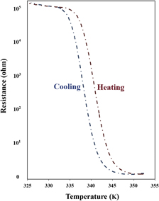
 $(001)[010]_{{\rm{YSZ}}} \parallel (111)[00\overline 1 ]_{{\rm{NiO}}} $. The epitaxial relationship at the NiO/VO2 interface was determined to be $(010)[001]_{{\rm{VO2}}} \parallel (111)[00\overline 1 ]_{{\rm{NiO}}} $. The SMT characteristics of these fully relaxed films were determined, and a transition temperature of 341 K with amplitude over four orders of magnitude and the hysteresis of 3.4 K hysteresis were obtained, which are close to those of the bulk high quality single crystals.