Hostname: page-component-745bb68f8f-v2bm5 Total loading time: 0 Render date: 2025-01-15T23:03:26.794Z Has data issue: false hasContentIssue false

Adsorption on epitaxial graphene on SiC(0001)

Published online by Cambridge University Press:  11 September 2013

Han Huang*
Affiliation:
Institute of Super-Microstructure and Ultrafast Process in Advanced Materials, School of Physics and Electronics, Central South University, China, 410083; Department of Physics, National University of Singapore, Singapore, 117542; and Graphene Research Center, National University of Singapore, Singapore 117546
Andrew Thye Shen Wee*
Affiliation:
Department of Physics, National University of Singapore, Singapore, 117542; and Graphene Research Center, National University of Singapore, Singapore 117546
*
a)Address all correspondence to these authors. e-mail: physhh@csu.edu.cn
Get access

Abstract

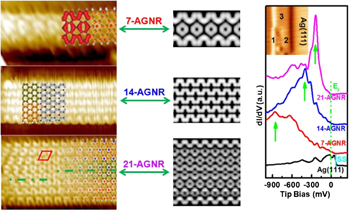
Graphene, a single atomic sheet of sp2-bonded carbon atoms arranged in a honeycomb lattice, exhibits extraordinary electrical and mechanical properties, attracting much attention in both academia and industry. The preparation of high quality large-area graphene and the tuning of graphene electronic properties are important topics in this field. In this feature paper, we review our recent work on epitaxial graphene (EG) on SiC(0001). First, we introduce the bottom-up growth mechanism of the first few EG layers on SiC(0001), and the modification of graphene electronic properties by means of surface transfer doping with electron withdrawing materials (F4-TCNQ and MoO3). Next, we summarize the adsorption behaviors of organic (PTCDA, ClAlPc, and C60F48) and inorganic (bismuth) materials on EG/SiC(0001). Finally, as an example of tuning the electronic properties of graphene by reducing its dimensionality, we demonstrate the molecular self-assembly of atomically precise armchair graphene nanoribbons with varying widths and electronic structures.

Type
Invited Papers
Copyright
Copyright © Materials Research Society 2013 

Access options

Get access to the full version of this content by using one of the access options below. (Log in options will check for institutional or personal access. Content may require purchase if you do not have access.)

References

REFERENCES

Geim, A.K. and Novoselov, K.S.: The rise of graphene. Nat. Mater. 6, 183 (2007).Google Scholar
Geim, A.K.: Graphene: Status and prospects. Science 324, 1530 (2009).CrossRefGoogle ScholarPubMed
Castro Neto, A.H., Guinea, F., Peres, N.M.R., Novoselov, K.S., and Geim, A.K.: The electronic properties of graphene. Rev. Mod. Phys. 81, 109 (2009).Google Scholar
Novoselov, K.S., Geim, A.K., Morozov, S.V., Jiang, D., Zhang, Y., Dubonos, S.V., Grigorieva, I.V., and Firsov, A.A.: Electric field effect in atomically thin carbon films. Science 306, 666 (2004).CrossRefGoogle ScholarPubMed
Chen, W., Xu, H., Liu, L., Gao, X.Y., Qi, D.C., Peng, G.W., Tan, S.C., Feng, Y.P., Loh, K.P., and Wee, A.T.S.: Atomic structure of the 6H-SiC(0001) nanomesh. Surf. Sci. 596, 176 (2005).CrossRefGoogle Scholar
Chen, W., Chen, S., Qi, D.C., Gao, X.Y., and Wee, A.T.S.: Surface transfer p-type doping of epitaxial graphene. J. Am. Chem. Soc. 129, 10418 (2007).Google Scholar
Chen, W. and Wee, A.T.S.: Self-assembly on silicon carbide nanomesh templates. J. Phys. D: Appl. Phys. 40, 6287 (2007).CrossRefGoogle Scholar
Gao, X.Y., Chen, S., Liu, T., Chen, W., Wee, A.T.S., Nomoto, T., Yagi, S., Soda, K., and Yuhara, J.: Disorder beneath epitaxial graphene on SiC(0001): An x-ray absorption study. Phys. Rev. B 78, 201404 (2008).Google Scholar
Poon, S.W., Chen, W., Tok, E.S., and Wee, A.T.S.: Probing epitaxial growth of graphene on silicon carbide by metal decoration. Appl. Phys. Lett. 92, 104102 (2008).CrossRefGoogle Scholar
Huang, H., Chen, W., Chen, S., and Wee, A.T.S.: Bottom-up growth of epitaxial graphene on 6H-SiC(0001). ACS Nano 2, 2513 (2008).Google Scholar
Gao, X.Y., Chen, S., Liu, T., Chen, W., Wee, A.T.S., Nomoto, T., Yagi, S., Soda, K., and Yuhara, J.: Si clusters on reconstructed SiC (0001) revealed by surface extended x-ray absorption fine structure. Appl. Phys. Lett. 95, 144102 (2009).CrossRefGoogle Scholar
Chen, W., Qi, D.C., Gao, X.Y., and Wee, A.T.S.: Surface transfer doping of semiconductors. Prog. Surf. Sci. 84, 279 (2009).Google Scholar
Huang, H., Chen, S., Gao, X.Y., Chen, W., and Wee, A.T.S.: Structural and electronic properties of PTCDA thin films on epitaxial graphene. ACS Nano 3, 3431 (2009).Google Scholar
Lu, Y.H., Chen, W., Feng, Y.P., and He, P.M.: Tuning the electronic structure of graphene by an organic molecules. J. Phys. Chem. B 113, 2 (2009)Google Scholar
Sun, J.T., Lu, Y.H., Chen, W., Feng, Y.P., and Wee, A.T.S.: Linear tuning of charge carriers in graphene by organic molecules and charge-transfer complexes. Phys. Rev. B 81, 155403 (2010).Google Scholar
Chen, S., Chen, W., Huang, H., Gao, X.Y., Qi, D.C., Wang, Y.Z., and Wee, A.T.S.: Template-directed molecular assembly on silicon carbide nanomesh: Comparison between CuPc and pentacene. ACS Nano 4, 849 (2010).Google Scholar
Chen, Z.Y., Santoso, I., Wang, R., Xie, L.F., Mao, H.Y., Huang, H., Wang, Y.Z., Gao, X.Y., Chen, Z.K., Ma, D.G., Wee, A.T.S., and Chen, W.: Surface transfer hole doping of epitaxial graphene using MoO3 thin film. Appl. Phys. Lett. 96, 213104 (2010).Google Scholar
Chen, W., Chen, S., Ni, Z.H., Huang, H., Qi, D.C., Gao, X.Y., Shen, Z.X., and Wee, A.T.S.: Band-bending at the graphene–SiC interfaces: Effect of the substrate. Jpn. J. Appl. Phys. 49, 01AH05 (2010).Google Scholar
Poon, S.W., Chen, W., Wee, A.T.S., and Tok, E.S.: Growth dynamics and kinetics of monolayer and multilayer graphene on a 6H-SiC(0001) substrate. Phys. Chem. Chem. Phys. 12, 13522 (2010).Google Scholar
Huang, H., Wong, S.L., Tin, C-C., Luo, Z.Q., Shen, Z.X., Chen, W., and Wee, A.T.S.: Epitaxial growth and characterization of graphene on free-standing polycrystalline 3C-SiC. J. Appl. Phys. 110, 014308 (2011).Google Scholar
Wong, S.L., Huang, H., Wang, Y.Z., Cao, L., Qi, D.C., Santoso, I., Chen, W., and Wee, A.T.S.: Quasi-free-standing epitaxial graphene on SiC (0001) by fluorine intercalation from a molecular source. ACS Nano 5, 7662 (2011).Google Scholar
Wong, S.L., Huang, H., Chen, W., and Wee, A.T.S.: STM studies of epitaxial graphene. MRS Bull. 37, 11951202 (2012).Google Scholar
Huang, H., Wong, S.L., Sun, J.T., Chen, W., and Wee, A.T.S.: Trapping single polar molecules in SiC nanomesh via out-of-plane dipoles. ACS Nano 6, 2774 (2012).Google Scholar
Sun, J.T., Huang, H., Wong, S.L., Gao, H-J., Feng, Y.P., and Wee, A.T.S.: Energy-gap opening in a Bi(110) nanoribbon induced by edge reconstruction. Phys. Rev. Lett. 109, 246804 (2012).CrossRefGoogle Scholar
Huang, H., Wei, D.C., Sun, J.T., Wong, S.L., Feng, Y.P., Castro Neto, A.H., and Wee, A.T.S.. Spatially resolved electronic structures of atomically precise armchair graphene nanoribbons. Sci. Rep. 2, 983 (2012).Google Scholar
Yu, X.J., Wilhelmi, O., Moser, H.O., Vidyaraj, S.V., Gao, X.Y., Wee, A.T.S., Nyunt, T., Qian, H.J., and Zheng, H.W.: New soft x-ray facility SINS for surface and nanoscale science at SSLS. J. Electron. Spectrosc. Relat. Phenom. 144, 1031 (2005).Google Scholar
Novoselov, K.S., Jiang, D., Schedin, F., Booth, T.J., Khotkevich, V.V., Morozov, S.V., and Geim, A.K.: Two-dimensional atomic crystals. Proc. Natl. Acad. Sci. U.S.A. 102, 10451 (2005).Google Scholar
Li, X.L., Zhang, G.Y., Bai, X.D., Sun, X.M., Wang, X.R., Wang, E., and Dai, H.J.: Highly conducting graphene sheets and Langmuir-Blodgett films. Nat. Nanotechnol. 3, 538 (2008).Google Scholar
Land, T.A., Michely, T., Behm, R.J., Hemminger, J.C., and Comsa, G.: STM investigation of single layer graphite structures produced on Pt(111) by hydrocarbon decomposition. Surf. Sci. 264, 261 (1992).Google Scholar
Nagashima, A., Nuka, K., Itoh, H., Ichinokawa, T., Oshima, C., and Otani, S.: Electronic states of monolayer graphite formed on TiC(111) surface. Surf. Sci. 291, 93 (1993).Google Scholar
Bae, S., Kim, H., Lee, Y., Xu, X.F., Park, J.S., Zheng, Y., Balakrishnan, J., Lei, T., Kim, H.R., Song, Y.I., Kim, Y.J., Kim, K.S., Ozyilmaz, B., Ahn, J.H., Hong, B.H., and Iijima, S.: Roll-to-roll production of 30-inch graphene films for transparent electrodes. Nat. Nanotechnol. 5, 574 (2010).Google Scholar
Li, X.S., Cai, W.W., Colombo, L., and Ruoff, R.S.: Evolution of graphene growth on Ni and Cu by carbon isotope labeling. Nano Lett. 9, 4268 (2009).CrossRefGoogle ScholarPubMed
Elena, L., Norman, C.B., Peter, J.F., and Kevin, F.M.: Evidence for graphene growth by C cluster attachment. New J. Phys. 10, 093026 (2008).Google Scholar
Sutter, P.W., Flege, J-I., and Sutter, E.A.: Epitaxial graphene on ruthenium. Nat. Mater. 7, 406 (2008).CrossRefGoogle ScholarPubMed
Reina, A., Jia, X., Ho, J., Nezich, D., Son, H., Bulovic, V., Dresselhaus, M.S., and Kong, J.: Large area, few-layer graphene films on arbitrary substrates by chemical vapor deposition. Nano Lett. 9, 30 (2008).Google Scholar
Coraux, J., N'Diaye, A.T., Engler, M., Busse, C., Wall, D., Buckanie, N., Heringdorf, F., van Gastel, R., Poelsema, B., and Michely, T.: Growth of graphene on Ir(111). New J. Phys. 11, 023006 (2009).CrossRefGoogle Scholar
Berger, C., Song, Z.M., Li, T.B., Li, X.B., Ogbazghi, A.Y., Feng, R., Dai, Z.T., Marchenkov, A.N., Conrad, E.H., First, P.N., and de Heer, W.A.: Ultrathin epitaxial graphite: 2D electron gas properties and a route toward graphene-based nanoelectronics. J. Phys. Chem. B 108, 19912 (2004).Google Scholar
Emtsev, K.V., Bostwick, A., Horn, K., Jobst, J., Kellogg, G.L., Ley, L., McChesney, J.L., Ohta, T., Reshanov, S.A., Rohrl, J., Rotenberg, E., Schmid, A.K., Waldmann, D., Weber, H.B., and Seyller, T.: Towards wafer-size graphene layers by atmospheric pressure graphitization of silicon carbide. Nat. Mater. 8, 203 (2009).Google Scholar
Bostwick, A., McChesney, J., Ohta, T., Rotenberg, E., Seyller, T., and Horn, K.: Experimental studies of the electronic structure of graphene. Prog. Surf. Sci. 84, 380 (2009).Google Scholar
First, P.N., de Heer, W.A., Seyller, T., Berger, C., Stroscio, J.A., and Moon, J-S.: Epitaxial graphenes on silicon carbide. MRS Bull. 35, 296 (2010).Google Scholar
Moon, J.S., Curtis, D., Bui, S., Hu, M., Gaskill, D.K., Tedesco, J.L., Asbeck, P., Jernigan, G.G., VanMil, B.L., Myers-Ward, R.L., Eddy, C.R., Campbell, P.M., and Weng, X.: Top-gated epitaxial graphene FETs on Si-Face SiC wafers with a peak transconductance of 600 mS/mm. IEEE Electron Device Lett. 31, 260 (2010).Google Scholar
Singh, R.S., Nalla, V., Chen, W., Wee, A.T.S., and Ji, W.: Laser patterning of epitaxial graphene for Schottky junction photodetectors. ACS Nano 5, 5969 (2011).Google Scholar
Nomani, M.W.K., Shishir, R., Qazi, M., Diwan, D., Shields, V.B., Spencer, M.G., Tompa, G.S., Sbrockey, N.M., and Koley, G.: Highly sensitive and selective detection of NO2 using epitaxial graphene on 6H-SiC. Sens. Actuators, B 150, 301 (2010).Google Scholar
Van Bommel, A.J., Crombeen, J.E., and Van Tooren, A.: LEED and Auger electron observations of the SiC(0001) surface. Surf. Sci. 48, 463 (1975).Google Scholar
Emtsev, K.V., Speck, F., Seyller, T., Ley, L., and Riley, J.D.: Interaction, growth, and ordering of epitaxial graphene on SiC(0001) surfaces: A comparative photoelectron spectroscopy study. Phys. Rev. B 77, 155303 (2008).Google Scholar
Lauffer, P., Emtsev, K.V., Graupner, R., Seyller, T., Ley, L., Reshanov, S.A., and Weber, H.B.: Atomic and electronic structure of few-layer graphene on SiC(0001) studied with scanning tunneling microscopy and spectroscopy. Phys. Rev. B 77, 155426 (2008).CrossRefGoogle Scholar
Gierz, I., Riedl, C., Starke, U., Ast, C.R., and Kern, K.: Atomic hole doping of graphene. Nano Lett. 8, 4603 (2008).Google Scholar
Giovannetti, G., Khomyakov, P.A., Brocks, G., Karpan, V.M., van den Brink, J., and Kelly, P. J.: Doping graphene with metal contacts. Phys. Rev. Lett. 101, 026803 (2008).Google Scholar
Garnica, M., Stradi, D., Barja, S., Calleja, F., Diaz, C., Alcami, M., Martin, N., Vazauez de Parga, A.L., Martin, F., and Miranda, R.: Long-range magnetic order in a purely organic 2D layer adsorbed on epitaxial graphene. Nat. Phys. 9, 368 (2013).Google Scholar
Wang, X.R., Tabakman, S.M., and Dai, H.J.: Atomic layer deposition of metal oxides on pristine and functionalized graphene. J. Am. Chem. Soc. 130, 8152 (2008).Google Scholar
Wang, Q.H., and Hersam, M.C.: Room-temperature molecular-resolution characterization of self-assembled organic monolayers on epitaxial graphene. Nat. Chem. 1, 206 (2009).Google Scholar
Dil, H., Lobo-Checa, J., Laskowski, R., Blaha, P., Erner, S., Osterwalder, J., and Greber, T.: Surface trapping of atoms and molecules with dipole rings. Science 319, 1824 (2008).Google Scholar
Varchon, F., Mallet, P., Veuillen, J.Y., and Magaud, L.: Ripples in epitaxial graphene on the Si-terminated SiC(0001) surface. Phys. Rev. B 77, 235412 (2008).Google Scholar
Kera, S., Yamane, H., Honda, H., Fukagawa, H., Okudaira, K.K., and Ueno, N.: Photoelectron fine structures of uppermost valence band for well-characterized ClAl-phthalocyanine ultrathin film: Ups and MAES study. Surf. Sci. 566, 571 (2004).Google Scholar
Riedl, C., Coletti, C., Iwasaki, T., Zakharov, A.A., and Starke, U.: Quasi-free-standing epitaxial graphene on SiC obtained by hydrogen intercalation. Phys. Rev. Lett. 103, 246804 (2009).CrossRefGoogle ScholarPubMed
Song, C.L., Wang, Y.L., Jiang, Y.P., Zhang, Y., and Chang, C.Z.: Topological insulator Bi2Se3 thin films grown on double-layer graphene by molecular beam epitaxy. Appl. Phys. Lett. 97, 143118 (2010).Google Scholar
Son, Y.W., Cohen, M.L., and Louie, S.G.: Energy gaps in graphene nanoribbons. Phys. Rev. Lett. 97, 216803 (2006).Google Scholar
Cai, J.M., Ruffieux, P., Jaafar, R., Bieri, M., Braun, T., Blankenburg, S., Muoth, M., Seitsonen, A.P., Saleh, M., Feng, X.L., Mullen, K., and Fasel, R.: Atomically precise bottom-up fabrication of graphene nanoribbons. Nature 466, 470 (2010).Google Scholar
Ruffieux, P., Cai, J.M., Plumb, N.C., Patthey, L., Prezzi, D., Ferretti, A., Molinari, E., Feng, X.L., Mullen, K., Pignedoli, C.A., and Fasel, R.: Electronic structure of atomically precise graphene nanoribbons. Acs Nano 6, 6930 (2012).Google Scholar
Koch, M., Ample, F., Joachim, C., and Grill, L.: Voltage-dependent conductance of a single graphene nanoribbon. Nat. Nanotechnol. 7, 713 (2012).Google Scholar
Linden, S., Zhang, D., Timmer, A., Aghdassi, N., Franke, J.H., Zhang, H., Feng, X., Mullen, K., Fuchs, H., Chi, L., and Zacharias, H.: Electronic structure of specially aligned graphene nanoribbons on Au(788). Phys. Rev. Lett. 108, 216801 (2012).Google Scholar
Odom, T.W., Huang, J.L., Kim, P., and Lieber, C.M.: Atomic structure and electronic properties of single-walled carbon nanotubes. Nature 391, 62 (1998).Google Scholar
Clair, S., Kim, Y., and Kawai, M.: Energy level alignment of single-walled carbon nanotubes on metal surfaces. Phys. Rev. B 83, 245422 (2011).CrossRefGoogle Scholar