I. INTRODUCTION
Energy is one of the most important core requirements for the progress of modern civilization. As of today, most of our energy demand is fulfilled by the supply of fossil fuels. Burning the fossil fuels for energy generation has been shown to be one of the reasons behind global warming and climate change. Interestingly, only one-third of the primary energy input is utilized efficiently, and two-third of it is wasted in the form of heat.Reference He, Kanatzidis and Dravid1,Reference Ovik, Long, Barma, Riaz, Sabri, Said and Saidur2 Hence, it is desirable to develop an energy conversion device that can produce electricity using the huge amount of waste heat generated from automotive exhausts, industrial processes, and residential heating. Thermoelectric (TE) power generation offers a fascinating prospect as it transforms thermal energy (waste heat) into electrical energy using the Seebeck effect. Moreover, it is a solid-state device without any moving parts, offering great flexibility in operational integration.Reference Ullah, Saidur, Ping, Akikur and Shuvo3,Reference Tie and Tan4 The performance of a TE device is generally evaluated by a figure-of-merit called ZT, which corresponds to the intrinsic properties of the material as expressed by the following equation:
where S is the Seebeck coefficient, σ is the electric conductivity, κ is the thermal conductivity, and T is the temperature. Thermal conductivity has a contribution from two parameters namely electrical thermal conductivity (κe) and lattice thermal conductivity (κl). A good TE material with a high ZT value requires a high Seebeck coefficient (S), high electrical conductivity (σ), and low lattice thermal conductivity (κ). The primary obstacle to increase ZT is that these fundamental properties of materials are interconnected. As a result, enhancing one property deteriorates the others.
Conventional TE materials are based on chalcogenides such as Bi2Te3,Reference Scheele, Oeschler, Meier, Kornowski, Klinke and Weller5 Sb2Te3,Reference Poudel, Hao, Ma, Lan, Minnich, Yu, Yan, Wang, Muto and Vashaee6 Zn4Sb3,Reference Caillat, Fleurial and Borshchevsky7 Bi2Se3,Reference Kadel, Kumari, Li, Huang and Provencio8 and SnTe.Reference Brebrick and Strauss9 However, most of the waste heat generated from various sources is >900 K and these materials decompose and oxidize at such high temperatures. Oxides are a better alternative for high-temperature TE applications due to their low costs, and higher oxidation resistance with better thermal stability.
Recently oxide TE materialsReference Takeuchi, Kondo, Takami, Takahashi, Ikuta, Mizutani, Soda, Funahashi, Shikano and Mikami10,Reference Van Nong, Pryds, Linderoth and Ohtaki11 such as NaxCoO2, Ca3Co4O9, etc. showed good ZT values with p-type conductivity. However, their ZT values are not comparable with the conventional chalcogenides. Besides, there are not many options available among oxide-based materials, to choose as n-type element in the TE module. It is beneficial to have both n-type and p-type oxides with good ZT values to reduce the strain mismatch in the TE module in which n-type and p-type materials are connected thermally in parallel and electrically in series.Reference Snyder and Toberer12 In recent years, Nb and La-doped SrTiO3 perovskite-based n-type materials showed very promising high-temperature TE properties, but their ZT values need to be improved to be considered for commercialization.
In the present work, we hypothesize that SrTiO3-based double perovskites (Sr2TiB′O6) are environmentally friendly high-temperature TE materials. Double perovskite materials were extensively investigated over the years for their wide range of exciting properties,Reference Sarma, Sampathkumaran, Ray, Nagarajan, Majumdar, Kumar, Nalini and Row36–Reference Meetei, Erten, Mukherjee, Randeria, Trivedi and Woodward40 e.g., colossal magneto-resistance, ferroelectricity, multiferroicity, high T c superconductivity, multi-band Mott insulators, and half-metallic behavior. A2B2O6 double perovskites are very amenable to compositional modification, whereby using different types of B site cations, their electrical, magnetic, and thermal properties can be tailored. Furthermore, these materials have complex crystal structure capable of accommodating multiple cations, which can act as phonon scattering centers required for low lattice thermal conductivity. Although some papers reportedReference Aguirre, Logvinovich, Bocher, Robert, Ebbinghaus and Weidenkaff13–Reference Smith, Sleight and Subramanian15,Reference Sugahara, Van Nong and Ohtaki17,Reference Sugahara, Ohtaki and Suganuma18 on TE properties of double perovskites as presented in Table I, most of these materials were primarily designed for investigating magnetoresistance, mutiferroics properties.
TABLE I. TE properties such as electrical conductivity, Seebeck coefficient, power factor, and ZT of different oxide TE materials.
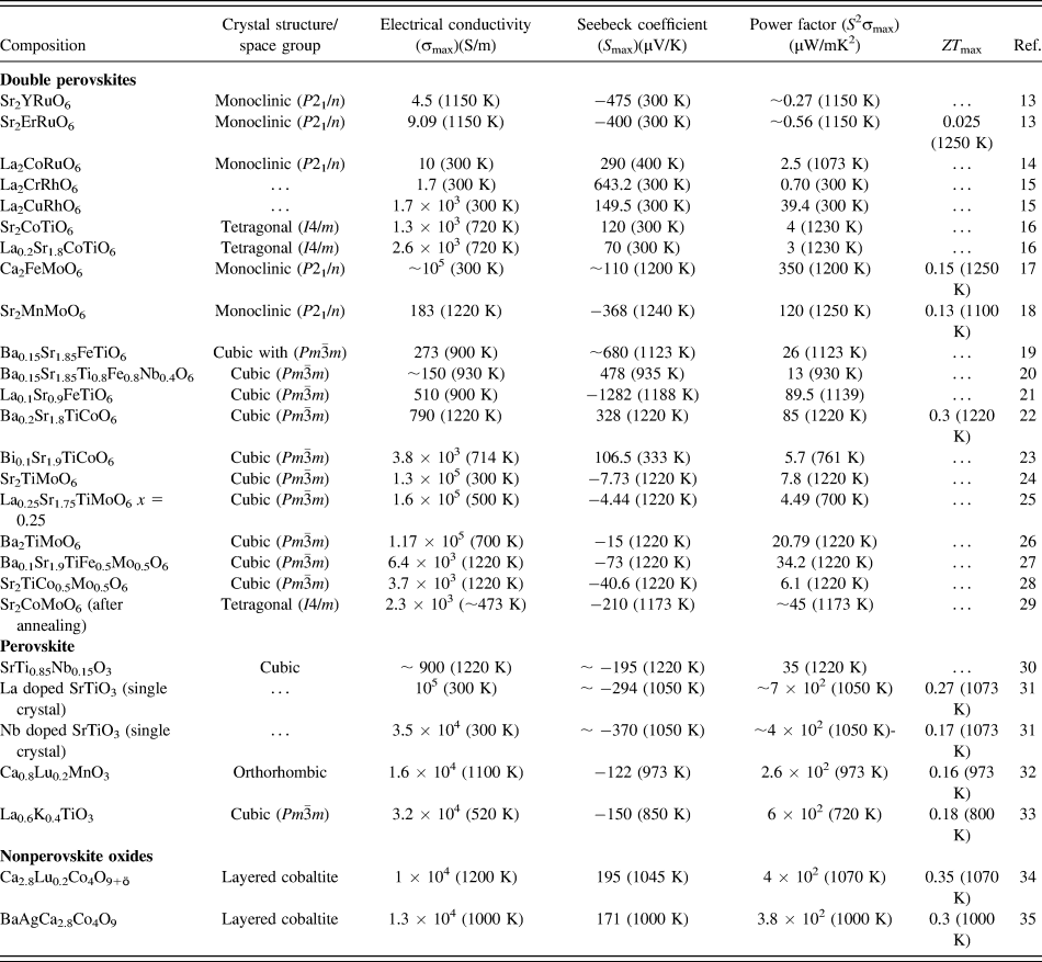
Recently, we published a series of papers on SrTiO3-based double perovskites for high-temperature TE application. We showed that by selecting appropriate elements for A-site and B-site cations in A2B2O6 double perovskite and manipulating the dopant concentrations along with optimized processing parameters,Reference Saxena, Tanwar and Maiti24,Reference Saxena and Maiti25 one can achieve very large thermopower,Reference Roy, Waghmare and Maiti19,Reference Saxena, Roy, Acharya, Bose, Tanwar and Maiti22,Reference Roy, Bose and Maiti41 metal-like electrical conductivity,Reference Saxena, Tanwar and Maiti24–Reference Saxena and Maiti26 and glass-like thermal conductivity.Reference Saxena, Roy, Acharya, Bose, Tanwar and Maiti22 In this article, we present a comprehensive review on the recent progress of Sr2B′B″O6-based double perovskites for high-temperature TE applications and the future direction. We demonstrated that using glassy state of relaxor ferroelectrics above the Burns temperature can be instrumental in achieving very low thermal conductivity in these double perovskites to enhance the ZT values. Moreover, we discovered a new class of oxide materials exhibiting temperature driven p–n type resistance switching behavior coupled with a large change in thermopower, which can pave way for the fabrication of novel high temperature multifunctional devices.
II. DESIGN OF DOUBLE PEROVSKITES
Double perovskites have stoichiometric formula A2B′B″O6, where the B-sites, i.e., B′, B″ can be occupied by the different combination of transition metals.Reference Howard, Kennedy and Woodward42,Reference Anderson, Greenwood, Taylor and Poeppelmeier43 The crystal structure and space group of double perovskites mainly depend on the arrangement of B′O6 and B″O6 octahedra, especially their ordering and tilting.Reference King and Woodward44 There are three types of B-site cationic arrangements in the 3-dimensional crystal structure, i.e., random, rock salt, and layered arrangement.Reference Anderson, Greenwood, Taylor and Poeppelmeier43 The space-group of double perovskites with randomly ordered octahedra is generally ![]() $Pm\bar{3}m$, as shown schematically in Fig. 1(a). In the unit cell of a randomly ordered (
$Pm\bar{3}m$, as shown schematically in Fig. 1(a). In the unit cell of a randomly ordered (![]() $Pm\bar{3}m$) double perovskite, the corner positions are occupied by A-site (0, 0, 0) divalent cations. However, B-site tetravalent cations (B′ and B″) are placed in the body centered position (1/2, 1/2, 1/2) and oxygen anions sit at the face-centered positions (1/2, 1/2, 0). On the contrary, in double perovskite structure with rock salt ordering, B′O6 and B″O6 octahedra are alternatively arranged in three-dimension space resulting different space groups, such as
$Pm\bar{3}m$) double perovskite, the corner positions are occupied by A-site (0, 0, 0) divalent cations. However, B-site tetravalent cations (B′ and B″) are placed in the body centered position (1/2, 1/2, 1/2) and oxygen anions sit at the face-centered positions (1/2, 1/2, 0). On the contrary, in double perovskite structure with rock salt ordering, B′O6 and B″O6 octahedra are alternatively arranged in three-dimension space resulting different space groups, such as ![]() $Fm\bar{3}m$, I4/m, and P4/nmc. The least common crystal structure of the double perovskite is layered-type in which, the layers of B′O6 and B″O6 octahedra are alternately arranged only in one direction.
$Fm\bar{3}m$, I4/m, and P4/nmc. The least common crystal structure of the double perovskite is layered-type in which, the layers of B′O6 and B″O6 octahedra are alternately arranged only in one direction.
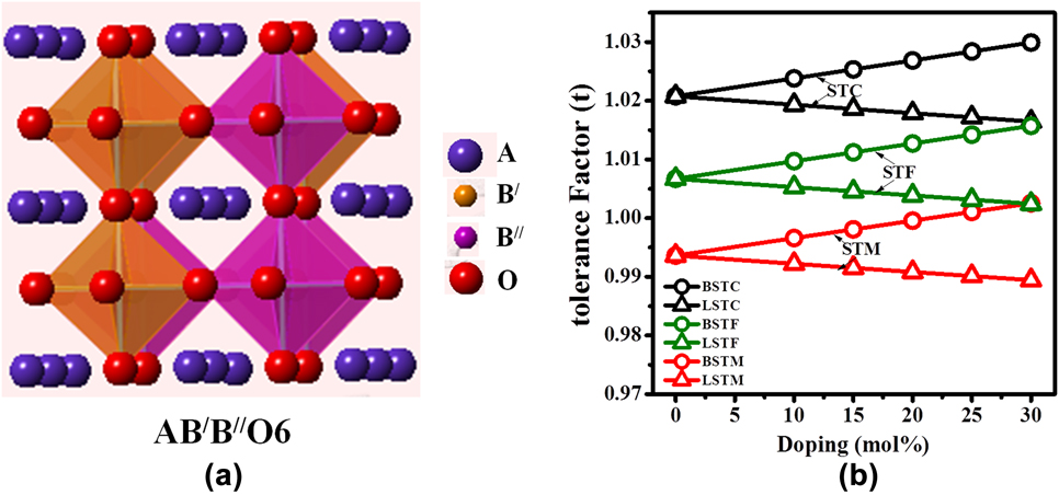
FIG. 1. (a) Schematic of A2B′B″O6 double perovskite structure and (b) tolerance factor of Ba and La-doped Sr2TiCoO6 (STC), Sr2TiFeO6 (STF), and Sr2TiMoO6 (STM).
Over the years, various types of perovskite materials were designed based on the Goldschmidt tolerance factor.Reference Goldschmidt45 Tolerance factor “t” is nearly 1 for cubic crystal structure. If the A-site cations have a smaller radius resulting in t < 1, cation size mismatch is generally compensated by tilting the BO6 octahedra. However, if t > 1, due to the larger radius of A-site ion, the mismatch is not offset by octahedral tilting, and a hexagonal phase may form. The equation for tolerance factorReference Anderson, Greenwood, Taylor and Poeppelmeier43 was further modified for our double perovskite structure, Ax′A2−xB′B″O6, where A′-cation was used as the dopant in the A-site. The modified equation for tolerance factor is given by the following equation:
 $$t = {{{{\left( x \right){r_{{\rm{A'}}}} + \left( {2 - x} \right){r_{\rm{A}}}} \over 2} + {r_{\rm{O}}}} \over {\sqrt 2 \left( {{{{r_{{\rm{B'}}}} + {r_{{\rm{B''}}}}} \over 2} + {r_{\rm{O}}}} \right)}}\quad ,$$
where, ![]() ${r_{\rm{A}}},\;{r_{{\rm{A'}}}},\;{r_{{\rm{B'}}}},\;{r_{{\rm{B''}}}},\;{\rm{and}}\;{r_{\rm{O}}}$ are the ionic radii of ions.
${r_{\rm{A}}},\;{r_{{\rm{A'}}}},\;{r_{{\rm{B'}}}},\;{r_{{\rm{B''}}}},\;{\rm{and}}\;{r_{\rm{O}}}$ are the ionic radii of ions.
To design the materials’ composition and dopant percentage, the tolerance factor [Eq. (2)] was calculated for Sr2TiMO6 double perovskites, where M = Fe, Co, and Mo. Tolerance factors with respect to the percentages of ‘A’-site doping for these double perovskite systems are plotted in Fig. 1(b). It is evident from the figure that pure Sr2TiCoO6 (STC) shows higher tolerance factor than Sr2TiMoO6 (STM) and Sr2TiFeO6 (STF) ceramics. Tolerance factor ‘t’ was found to increase with the substitution of Ba for the Sr-site in all the double perovskites such as STC, STF, and STM, whereas ‘t’ decreased with the La doping. Nevertheless, the tolerance factor values for all the compositions developed in the present work found to be within the range of 1 ± 0.03. It predicts that SrTiO3-based double perovskites are stable with a cubic crystal structure.
III. PROCESSING OF DOUBLE PEROVSKITES
In general, double perovskites are electrical insulators. However, in the TE applications, very good electrical conductivity of the material is desired. To engineer double perovskite oxides with reasonable electrical conductivity, it is essential to attain a single phase solid solution. The presence of impurities or secondary phase deteriorates the electrical conductivity. We used the solid-state reaction method in the present work to prepare solid solution of double perovskites. This method includes calcination of a homogeneous mixture of different powders such as oxides, carbonates, etc. This solid-state reaction process contains repeated grinding, milling, and sintering at high temperature. During sintering and calcination, various parameters such as temperature, heating/cooling rate, gas flow, etc. were optimized to acquire the required resultant phase of ceramic materials. There was another important step that we included in the current work, i.e., nanomilling of calcined powder. After nanomilling, the particle size of the starting powder for sintering was reduced to <100 nm. Smaller particle size is important to achieve the small grain size in the microstructure of the sample, which can enhance the phonon scattering at grain boundaries resulting in low lattice thermal conductivity (κl) of the ceramic materials. The calcined powder was milled by planetary micromill (Fritsch, PULVERISETTE 7 premium line, Rhineland Palatinate, Germany) at 600 rpm using zirconia grinding balls and ethanol as milling media. The schematic of the processing steps involved in the fabrication of double perovskite ceramics by the solid-state reaction method is presented in Fig. 2.
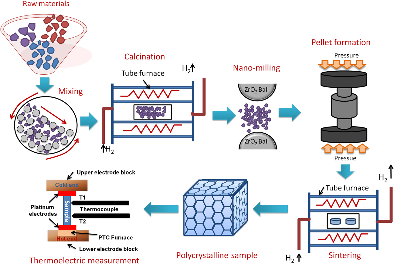
FIG. 2. Schematic of processing double perovskite ceramics by the solid-state reaction method and its TE measurement.
A. Effect of processing atmosphere
To obtain good electrical conductivity, we used transition metals with multiple oxidation states in the B-site of the double perovskite, which has the formal valence of +4. Hence, unwanted secondary phases might form in the system. In calcination and sintering, the processing atmosphere, i.e., inert (Ar, N2), oxidizing (Air) and reducing (H2) play a significant role in the formation of a single phase. Initially, we calcined and sintered La- and Ba-doped Sr2TiMoO6 in air. To analyze the phase purity and crystal structure of calcined and sintered sample, X-ray diffraction (XRD) was carried out by using a PANanalytical Empyrean ACMS 101 (Malvern Panalytical Ltd., Malvern, United Kingdom) diffractometer at room temperature. The XRD pattern of calcined and sintered powder showed that solid state reactions were not completed in air. We found a secondary phase, SrMoO4, as confirmed by the XRD profile in Fig. 3(a). SrMoO4 phase segregation suggests that Mo is more stable with +6 oxidation state as depicted by Eq. (3). The SrMoO4 phase exhibits insulating behavior and significantly reduces the overall conductivity of the system. However, Mo has a formal valence of (+4) in the double perovskite structure. To troubleshoot this problem, repeated process of grinding followed by calcination was carried out in reducing atmosphere as described by Eq. (4). Single-phase solid solution was achieved when calcination and sintering were carried out in reducing atmosphere, as shown in Fig. 3(a). To the best of our knowledge, there was no report on STM-based double perovskites demonstrating single-phase solid solution. Therefore, the sintering temperature, as well as the atmosphere, played significant role in the fabrication of these double perovskites.
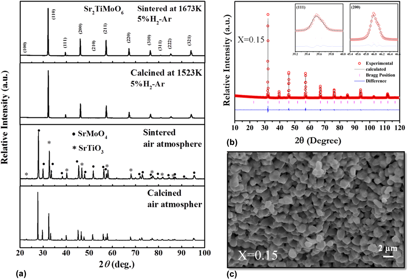
FIG. 3. (a) XRD pattern of STM powder calcined and sintered sample in the air and reducing atmospheres, (b) Rietveld analysis, and (c) SEM image of the fracture surface of the LSTM x = 0.15 ceramic sample. Reproduced from Reference Saxena and MaitiRef. 25 with permission from The Royal Society of Chemistry.
To determine the crystal structure of double perovskite oxides, Rietveld refinement of room temperature powder XRD data was carried out using Full Prof ProgramReference Rodríguez-Carvajal46 for all the double perovskite samples. We obtained a single-phase cubic symmetry for all the SrTiMO6 double perovskites, where M = Co, Mo, and Fe. The observed (open circle), calculated (continuous line), and the difference profiles obtained after refinement of the XRD pattern of LSTM x = 0.1 are shown in Fig. 3(b). The XRD data show a well-fitted graph with respect to ![]() $Pm\bar{3}m$ space group with very low-value of χ2 (1.41), which signifies the goodness of fit in the Rietveld refinement.Reference Saxena and Maiti25
$Pm\bar{3}m$ space group with very low-value of χ2 (1.41), which signifies the goodness of fit in the Rietveld refinement.Reference Saxena and Maiti25
The microstructure of all the ceramic samples (∼95–97% density) was analyzed by scanning electron microscopy (SEM) (Carl Zeiss GmbH, EV050, Oberkochen, Germany). All the double perovskite ceramic samples showed well-sintered, dense microstructure, as shown in Fig. 3(c) for LSTM.Reference Saxena and Maiti25 These double perovskites demonstrated a wide range of grain size distribution scaling from nm to μm range. Due to nanoscale high energy ball milling of calcined powder, we obtained a significant amount of grain size <500 nm reduction.
B. Effect of annealing
We studied the effect of annealing on the TE properties of Sr2CoMoO6-based double perovskite oxide.Reference Tanwar, Saxena and Maiti29 Figure 4 shows the structural and TE properties of as-sintered Sr2CoMoO6 (SCMO) oxide in comparison with SCMO sample annealed in reducing atmosphere. XRD of air-sintered SCMO implied the signature of a small concentration of nonperovskite phase SrMoO4, as shown in Fig. 4(a). Furthermore, we carried out the Rietveld refinement using Fullprof program to reveal the crystal structure and weight percentage of Sr2CoMoO6 and SrMoO4 phase of the air sintered sample. The Sr2CoMoO6 and SrMoO4 were fitted with I4/m and I4/a space group, respectively. However, the amount of this SrMoO4 secondary phase was found to be 8.9 wt%. To reduce the amount of the SrMoO4 phase, heat treatment was carried out in reducing atmosphere at 1273 K for 2 h. After annealing, there was an absence of SrMoO4 phase, as shown in Fig. 4(b). However, the extra peaks corresponding to the SrMoO3 perovskite phase was also recorded. The annealing process not only changed the phase of the system but also showed the effect on the microstructure of SCMO ceramic. Before annealing, all the grains were distinguished with clearly defined grain boundaries, as shown in Fig. 4(c). However, the microstructure of SCMO after annealing demonstrated molten phase with micron-scale grain.Reference Tanwar, Saxena and Maiti29
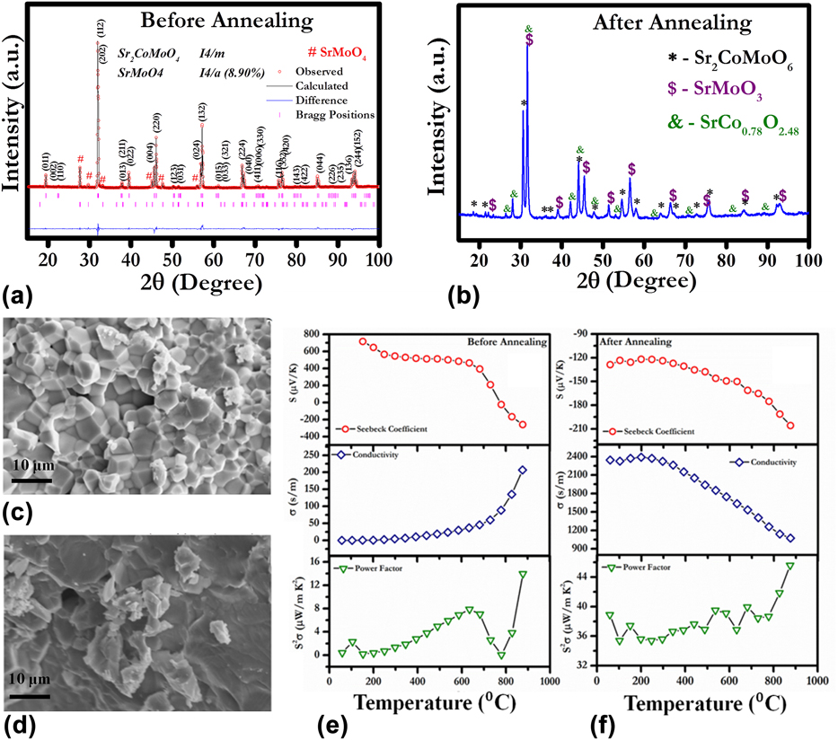
FIG. 4. (a) and (b) XRD, (c) and (d) SEM, (e) and (f) TE properties for SCMO ceramics before and after annealing, respectively. Reproduced from Reference Tanwar, Saxena and MaitiRef. 29 with the permission of AIP Publishing.
Annealing of SCMO ceramic in reducing atmosphere affected its TE properties significantly. Air-sintered SCMO ceramic exhibited insulator like behavior up to 913 K (∼0.2 S/m at room temperature) with p-type Seebeck coefficient, as shown in Fig. 4(e). Around 913 K, a sharp decrease in the Seebeck coefficient (S) was found and SCMO showed p–n type transition depicted in Fig. 4(e). After annealing, SCMO demonstrated n-type conduction behavior in the entire temperature range, as shown in Fig. 4(f). Furthermore, electrical conductivity was enhanced by ten times after annealing. With increasing temperature, electrical conductivity was decreased indicating the metal-like behavior. The maximum power factor (S 2σ) value, ∼45 µW/mK2, was achieved at 1173 K, which is significantly higher as compared to air-sintered SCMO ceramics (∼13 µW/mK2 at 1173 K).Reference Tanwar, Saxena and Maiti29 Hence, annealing was found to be an interesting way to enhance the electrical conductivity of any n-type TE materials and to improve the overall performance. The conduction mechanism of air-sintered and annealed sample was further explained by the following defect reactions:
The B-site cation in double perovskite oxides possesses formal valance of 4+. Hence, the B-site occupancy by Co3+ and Co2+ produces the oxygen vacancies as expressed by defect reactions (5) and (6). These oxygen vacancies are the sources of the positive charge carriers in the SCMO sample. However, the presence of Mo6+ in SCMO donates negative charge carrier, electron as depicted by Eq. (7). Hence the presence of both low mobility oxygen vacancies and high mobility electrons are expected to exist in the SCMO system. The p-type conduction observed till 1023 K in the air-sintered sample suggests the presence of positively charged oxygen vacancies as majority charge carriers. The air-sintered sample showed the presence of SrMoO4 as the secondary phase, which was reported as insulating in nature.Reference Maji, Jena, Asuvathraman and Kutty47 It validates the low electrical conductivity observed in the as-sintered sample. Moreover, at low temperature, electrons produced by defect reaction (7) are expected to be localized at defect sites in the ceramic sample. To overcome the energy barrier, the charge carriers (e−) required the activation energy for delocalization. Small polaron hopping phenomena were foundReference Tanwar, Saxena and Maiti29 to be the conductivity mechanism in SCMO. With increasing temperature, these electrons were expected to become delocalized contributing to the conductivity. The n-type conductivity observed in SCMO above 1023 K suggests the high mobility electrons as majority charge carriers, which further corroborates the higher conductivity values obtained beyond 1023 K. On the other hand, the SrMoO3 phase found in the annealed sample was reported to be metallic in nature.Reference Logvinovich, Aguiar, Robert, Trottmann, Ebbinghaus, Reller and Weidenkaff48 As a result the annealed sample showed higher conductivity values as well as metal-like (dσ/dT < 0) behavior in the temperature-dependent conductivity plot, as shown in Fig. 4(f) unlike the air-sintered SCMO sample.
IV. LARGE THERMOPOWER IN DOUBLE PEROVSKITES
For the potential TE materials, it is essential to have a high thermopower (S > 100 µV/K) in combination with a high value of electrical conductivity resulting in high TE power factor (S 2σ). In the present work, we engineered the SrTiO3-based double perovskite TE materials, Sr2TiB′O6, by using ferromagnetic elements (Co and Fe) at the B′-site, which resulted in double perovskites such as Sr2CoTiO6 (STC)Reference Saxena, Roy, Acharya, Bose, Tanwar and Maiti22 and Sr2FeTiO6 (STF).Reference Roy, Waghmare and Maiti19 Figure 5 shows the Seebeck coefficient and the electrical conductivity of these materials measured in the temperature range from 300 to 1200 K (ZEM-3 M10 apparatus, ADVANCE RIKO Inc., Yokohama, Japan). Both STF and STC compositions demonstrated positive Seebeck coefficient confirming the p-type behavior with holes as the dominant charge carriers. The Seebeck coefficient of STF was found to be higher than STC composition.
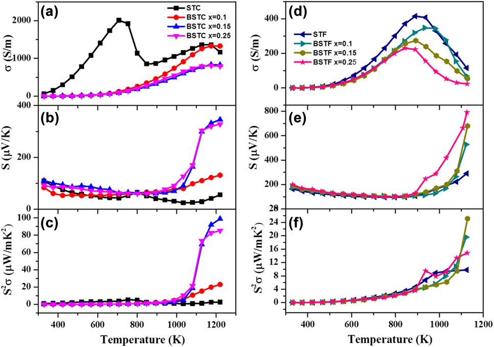
FIG. 5. TE properties such as (a) and (b) electrical conductivity, (c) and (d) Seebeck coefficient and (e) and (f) power factor of STC and STF-based TE materials. (a-c) reproduced from Ref. 22 with the permission of AIP Publishing and (d-f) reproduced from Reference Roy, Waghmare and MaitiRef. 19 with permission from The Royal Society of Chemistry.
Furthermore, we studied the effect of barium doping at A-site on TE properties of STC and STF. Doping of barium in the place of strontium increased the Seebeck coefficient of both STC and STF. Very large S value ∼800 μV/K at 1100 K was obtained in the Ba0.25Sr1.75TiFeO6 double perovskite. In the temperature-dependent conductivity curve, both STC and STF showed semiconductor (dσ/dT > 0) to metal-like (dσ/dT < 0) transition as evident in Figs. 5(a) and 5(d). Furthermore, the doping of Ba2+ at the Sr-site decreased the value of electrical conductivity in both STC and STF ceramics. Maximum conductivity value for STC was found to be higher than that of STF. The highest value of power factor (S 2σ) was found to be ∼100 μW/mK2 at 1200 K for BaxSr2−xTiCoO6 with x = 0.15 composition. In the pure STC sample, two semiconductors to metal transition peaks were found at 700 K and 1170 K, respectively, unlike the STF sample as shown in Fig. 5(a). The first semiconductor to metal transition temperature (T S–M) was found to be shifted to the higher temperature with the incorporation of Ba in the Sr-site. There could be a phase transition responsible for semiconductor to metal transition observed in STC. However, our laboratory scale high-temperature XRD did not show any peak splitting suggesting cubic phase in the whole temperature range of measurement. High-resolution XRD or neutron diffraction is required to unravel the possible phase transition in the STC sample. It is to be noted that these materials exhibited relaxor ferroelectricity as discussed in the subsequent section of this manuscript. Hence it is difficult to solve the crystal structure of BSTC since the metal–semiconductor transition temperatures belonged to the paraelectric region, which is known to possess the cubic crystal structure. Hence one may need to resolve the local structural ordering in this system.
Majority charge carriers (holes, h•) in STC and STF-based double perovskites can be explained by the charge compensation mechanism due to the substitution of B-site having formal charge +4 with multivalent cations such as Fe and Co. Defect reactions can be expressed by using Krӧger–Vink notation.
Due to the substitution of isovalent Ba2+ in the place of Sr2+ ions, no changes in charge carrier dynamics was expected, which explains p-type behavior observed in all the BSTC and BSTF compositions. However, the doping in A-site and B-site of double perovskite with metals having much higher oxidation state is expected to introduce e-s in these oxides. As a result, these double perovskites give rise to some new exciting behavior as discussed in a subsequent section.
V. DECOUPLING OF ‘PHONON-GLASS’ AND ‘ELECTRON-CRYSTAL’ BEHAVIOR IN OXIDES USING RELAXOR FERROELECTRIC INDUCED DIPOLAR SPIN GLASS
To achieve good ZT values in TE materials, it is essential to have high electrical conductivity and low thermal conductivity. It means that we need materials where electron transport in the medium should be as smooth as possible, but on the contrary, heat transport in the material should be as hard as possible. Slack summarized well this phenomenon by proposing “phonon glass electron crystal” model.Reference Slack and Rowe49 To determine the heat transport in the BSTC double perovskite, thermal diffusivity (D) and heat capacity (C p) were measured in the temperature range from 300 to 1273 K. The formula κ = ρC pD was used to calculate the thermal conductivity of these materials, where ρ is the density of samples. Thermal conductivity (κ) of all BSTC samples varies from 0.01 to 0.55 W/mKReference Saxena, Roy, Acharya, Bose, Tanwar and Maiti22, as shown in Fig. 6(a). Lattice thermal conductivity (κl) of the system was calculated by subtracting electronic thermal conductivity (κe) from total thermal conductivity (κ). Electronic thermal conductivity (κe) was calculated by using Wiedemann–Franz law, κe = LTσ, where L is the Lorentz number, σ is the electrical conductivity, and T is the temperature. Figure 6(b) shows the lattice thermal conductivity of BSTC ceramics. However, electronic thermal conductivity (κe) was found to be very small in this BSTC system. Thus, thermal conductivity of BSTC ceramics is primarily controlled by phonon transport (lattice thermal conductivity). Such glass-like low thermal conductivity is very beneficial to increase the figure of merit (ZT) and the performance of the TE device. The maximum value of ZT was obtained as ∼0.3 at 1220 K in BSTC with x = 0.2 composition, as shown in Fig. 6(c).
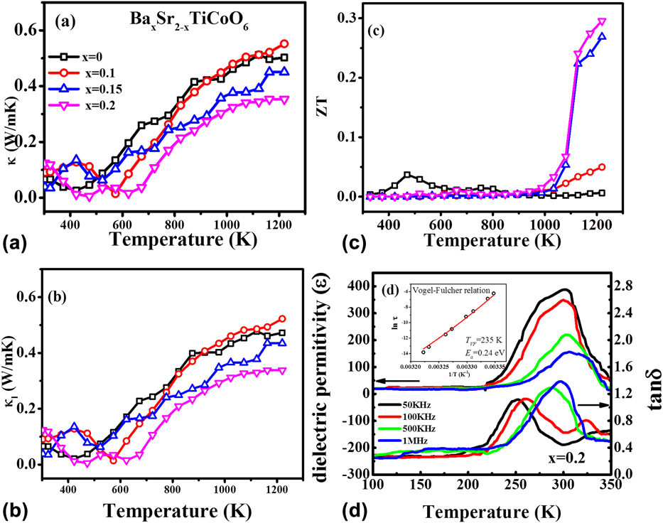
FIG. 6. Temperature dependence (a) thermal conductivity, (b) lattice thermal conductivity, (c) ZT of BaxSr2−xTiCoO6 ceramics with x = 0.0, 0.1, 0.15, and 0.2, (d) dielectric constant (ε) and tan δ of Ba0.2Sr1.8TiCoO6 ceramics and the inset shows the Vogel–Fulcher fitting. Reproduced from Reference Saxena, Roy, Acharya, Bose, Tanwar and MaitiRef. 22 with the permission of AIP Publishing.
However, the origin of such glass-like thermal conductivity in these BSTC double perovskites could not be explained by just considering phonon scattering due to small grain size and multiple cation sites. Moreover, the thermal conductivity of the BSTC sample was found to be continuously increasing with temperature till 1200 K, as shown in Fig. 6. This is opposite to what was observed for other TE materials, which showed a decrease in thermal conductivity with increase in temperature.Reference Aguirre, Logvinovich, Bocher, Robert, Ebbinghaus and Weidenkaff13,Reference Sugahara, Van Nong and Ohtaki17,Reference Wang, He, Li, Han and Zhang50,Reference Sugahara, Ohtaki and Souma51 However, the similar behavior of increasing thermal conductivity with temperature was found in the literature for the spin glass system.Reference Ackerman, Moy, Potter, Anderson and Lawless52,Reference Huang53 Interestingly, such thermal conductivity behavior was also reported in the relaxor ferroelectric material, which is known to behave like dipolar spin glass.Reference De Yoreo, Pohl and Burns54
Furthermore, we studied the dielectric behavior of BSTC ceramics to check if the material is relaxor indeed. The temperature dependence of dielectric constant (ε′) and loss tangent (tan δ) at various frequencies for all the BSTC compositions in the temperature range from 100 to 350 K is shown in Fig. 6(d). These materials showed relaxor behavior at low temperature, i.e., with increasing frequency dielectric permittivity, ε′decreased and the temperature of dielectric maxima was shifted toward higher temperatures. Also, these BSTC compositions were found to follow the modified Curie–Weiss law as described by the following equationReference Uchino and Nomura55:
where γ is called a degree of relaxation and its values lie between 1 and 2. The value γ = 1 shows that the Curie–Weiss law is valid for normal ferroelectric behavior. However, γ = 2 expresses the case of quadratic dependence suitable for an ideal relaxor ferroelectric.Reference Smolenskii and Agranovskaya56 The γ value obtained for this BSTC composition is 1.54, which suggests the ferroelectric relaxation behavior in these ceramics. Relaxor ferroelectrics are known to behave like dipolar glassReference Viehland, Jang, Cross and Wuttig57,Reference Viehland, Li, Jang, Cross and Wuttig58 where dipolar interactions of polar nanoregions (PNR) are thought to be responsible for relaxor behavior. However, at very high temperature, thermal fluctuations are so large that there are no such well-defined dipole moments and it exhibits glass-like behavior above Burns temperature (T D).Reference Burns and Dacol59–Reference Bhalla, Guo, Cross, Burns, Dacol and Neurgaonkar61 The Burns temperature (T D) value for BSTC with x = 0.2 composition was calculated to be 312 K at 100 kHz, which suggests that BSTC double perovskite becomes a glassy state above 312 K. The relaxation time (τ) for these relaxorsReference Shtrikman and Wohlfarth62–Reference Maiti, Guo and Bhalla64 can be estimated by Vogel–Fulcher law, which was originally derived for spin glass as described by the following equation:
where τ0 is the pre-exponential factor, E a is the activation energy for polarization fluctuations of an isolated cluster, k B is the Boltzmann constant, T m is the temperature corresponding to dielectric maxima, and T VF is the characteristic Vogel Fulcher freezing temperature. The temperature dependence of relaxation time of BSTC double perovskite was found to be well fitted with the Vogel Fulcher relation, as shown in the inset of Fig. 6(d) for Ba0.2Sr1.8TiCoO6 composition. It further justifies that these double perovskites behave like spin glass as a result of relaxor ferroelectricity. Moreover, these relaxors above Burns temperature (T D) behave like glass, which is the reason behind such low glass-like thermal conductivity observed in these double perovskite. Inducing dipolar glassy phase as a result of relaxor ferroelectricity in double perovskites can be a good strategy for decoupling ‘Phonon-Glass’ and ‘Electron Crystal’ behavior in oxides, which was considered as the bottleneck in the research of oxide TEs. Here we showed that using relaxor ferroelectrics above Burns temperature can produce glass-like thermal conductivity without affecting electrical conductivity much. To the best of our knowledge, this is the first material to demonstrate that decoupling of ‘Phonon Glass’ and ‘Electron Crystal’ behavior is possible in oxides.
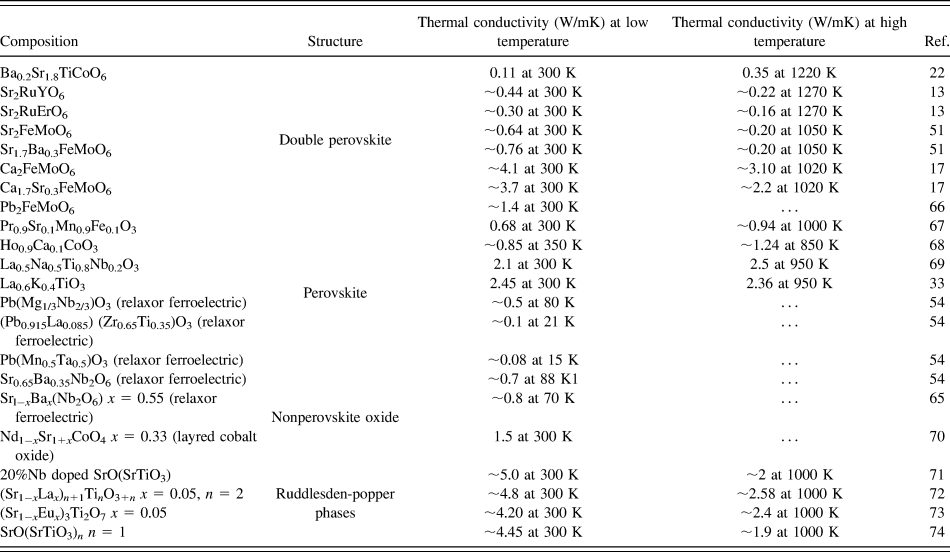
Furthermore, we compared the thermal conductivity of BSTC double perovskites with wide range of oxides such as double perovskites, single perovskites, layered oxide-like Ruddlesden–Popper phases and nonperovskite oxides, as summarized in Table II. It is evident that the thermal conductivity of the BSTC samples was found to be comparable with some double perovskites. However, it demonstrated lower thermal conductivity compared to other layered perovskite and nonperovskites. The trend in temperature-dependent thermal conductivity of BSTC ceramics was found to be similar to that what was reported for the relaxors ferroelectrics and spin glasses.Reference De Yoreo, Pohl and Burns54,Reference Fischer, Hässler and Hegenbarth65 However, we could not find any high-temperature studies on spin glasses as their thermal conductivity was studied primarily for other purposes such as magnetoresistance. Although some nonperovskite oxides showed a slightly increasing trend in thermal conductivity. However, there is no proper explanation for this behavior available in the literature. More theoretical as well as experimental analyses are required to understand the heat transport behavior in these double perovskites.
TABLE II. Thermal conductivity of different oxides.
VI. METAL-LIKE ELECTRICAL CONDUCTIVITY IN OXIDES
Both STC and STF materials discussed above showed good Seebeck coefficient. However, these materials suffered from low electrical conductivity (∼102 S/m) causing low power-factor obtained in these ceramics. Increasing the electrical conductivity of oxides is a daunting task because oxides are inherently insulator in nature. Recently, we developed Sr2TiMoO6 (STM)-based TE materialsReference Saxena, Tanwar and Maiti24 which demonstrated metal-like electrical conductivity (∼105 S/m). We also studied the effect of lanthanum and barium doping on AxSr2−xTiMoO6 based TE materials. Figure 7 shows TE properties like electrical conductivity (σ), Seebeck coefficient (S), and power factor (S 2σ) of AxSr2−xTiMoO6 (A = La, Ba) ceramic samples in the temperature range from 300 to 1273 K. Very high carrier concentration on the order of 1022 cm−3 was found in the Hall measurement of these double perovskites. The highest value of electrical conductivity, 1.64 × 10⁵ S/m, at 517 K was obtained for La0.25Sr1.75TiMoO6 composition, as shown in Fig. 7(a).
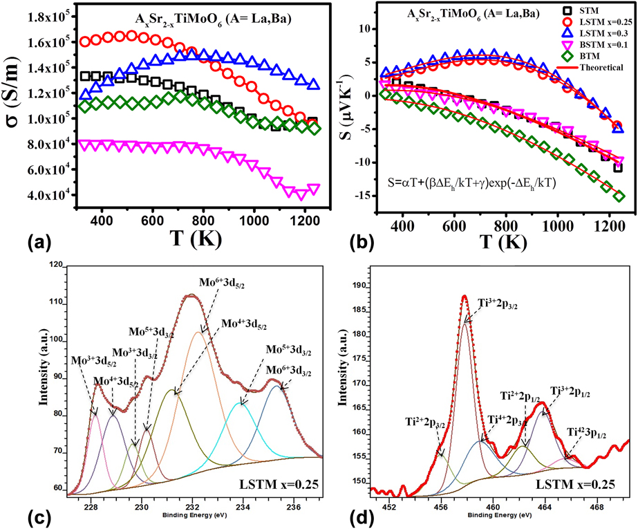
FIG. 7. TE properties: (a) electrical conductivity and (b) Seebeck coefficient of La- and Ba-doped STM ceramics with curve fitting and XPS analysis of (c) Mo and (d) Ti in LSTM with x = 0.25.
The Seebeck coefficient (S) of these materials showed temperature driven p-type to n-type conduction switching behavior. However, the p–n type switching temperature was found to be decreased with increasing Ba concentration in BSTM composition in contrary to LSTM, where the p–n transition temperature was increased due to La doping, as shown in Fig. 7. In the n-type region, Seebeck coefficient (S) for all the compositions was found to be increased with temperature. Although these STM-based double perovskites showed metallic behavior (dσ/dT < 0) in the temperature-dependent conductivity graph, they were not found to follow the degenerate Fermi gas model in the Seebeck coefficient due to localized Anderson transition.Reference Anderson75,Reference Bernasconi, Biaggio, Zgonik and Günter76 Generally, these kinds of perovskites with high carrier concentration (>1018 cm−3) are expected to show metal–insulator transition, as predicted by Mott criteria, ![]() $n_{\rm{e}}^{{1 / 3}}{a_0}\sim0.25$, where n e is the electronic carrier concentration and a 0 is the Bohr radius related with the carrier.Reference Cox77 As per the Mott criterion if the value exceeds 0.25, the conduction mechanism transforms from semiconductor to metallic.Reference Lee, Yang, Wilke, Trolier-McKinstry and Randall78 Since STM based double perovskites possess very high carrier concentration (1022 cm−3), they are expected to exhibit metallic behavior satisfying Mott criterion. However these STM-based compounds comprise transition metals like Ti and Mo, which are known to exist in multiple oxidation states. As a result, there can be a significant variation in the local electric fields and lattice distortions causing random electric field around the defect sites, resulting the charge carriers in the system localized, which is known as Anderson localization.Reference Anderson75,Reference Bernasconi, Biaggio, Zgonik and Günter76 As a result, these compounds do not follow the degenerate semiconductor model. To understand the charge transport mechanism in these complex oxides, it is essential to know the source of charge careers in these materials.
$n_{\rm{e}}^{{1 / 3}}{a_0}\sim0.25$, where n e is the electronic carrier concentration and a 0 is the Bohr radius related with the carrier.Reference Cox77 As per the Mott criterion if the value exceeds 0.25, the conduction mechanism transforms from semiconductor to metallic.Reference Lee, Yang, Wilke, Trolier-McKinstry and Randall78 Since STM based double perovskites possess very high carrier concentration (1022 cm−3), they are expected to exhibit metallic behavior satisfying Mott criterion. However these STM-based compounds comprise transition metals like Ti and Mo, which are known to exist in multiple oxidation states. As a result, there can be a significant variation in the local electric fields and lattice distortions causing random electric field around the defect sites, resulting the charge carriers in the system localized, which is known as Anderson localization.Reference Anderson75,Reference Bernasconi, Biaggio, Zgonik and Günter76 As a result, these compounds do not follow the degenerate semiconductor model. To understand the charge transport mechanism in these complex oxides, it is essential to know the source of charge careers in these materials.
From the temperature-dependent Seebeck coefficient measurement of these samples showing p–n type switching, it is imperative to have the coexistence of both positive and negative charge carriers in these compounds. Source of negative charge carriers can be explained by defect reaction (13) and (14) which suggests that La+3 inclusion in the place of Sr+2 and Mo+6 in Ti+4 site are the reason behind the generation of electrons. Besides, the electron generation due to oxygen vacancies is inherent defect reaction in oxides especially at high temperature as depicted by Eq. (10). However, both Mo and Ti present in STM double perovskites can exist at +3 oxidation state as well. The cause of positive charge carriers in these materials was considered to be +3 oxidation state of Mo and Ti occupying B-site of the double perovskite, which has formal valence +4 as expressed by Eq. (16).
where M = Mo, Ti.
Above defect reactions suggest that STM-based double perovskites can have the presence of electrons as well as positively charged oxygen vacancies. However, oxygen vacancies are known to have lower mobility as compared to electrons. Furthermore, the multiple oxidation states of Mo and Ti cations was confirmed by X-ray photoelectron spectroscopy (XPS; PHI 5000 Versaprobe II, ULVAC-PHI, Inc., Chigasaki, Japan) as shown in Figs. 7(c) and 7(d) for Mo 3d and Ti 2p spectra of LSTM x = 0.25. The XPS spectra confirmed the existence of Mo and Ti with multiple oxidation states. The obtained values of binding energies are very similar to the other reports in the literature.Reference Yang, Fung and Wang79–Reference Choi and Thompson82 XPS data suggest that the existence of Mo in +6 and +5 states enabled to reduce Ti even into +2 state, although in a little fraction of total Ti in the system. Mo3+, Ti3+, and Ti2+ were attributed to being the reason behind the positively charged oxygen vacancies. On the other hand, higher valence cations such as Mo5+ and Mo6+ generated the electrons.
Furthermore, we explained this p–n switching observed in the temperature-dependent Seebeck coefficient using an analytical model. In the case of coexisting electrons and holes, the total Seebeck coefficient ‘S’ was considered to be the sum of contribution from both types of charge carrier as given below.
Furthermore, the following equation can be derived:
where ΔE h is the activation energy for generation of positive charge carriers, σ0 and B are constant; k B is the Boltzmann constant, e is a charge of the electron, T is the temperature, E F is the Fermi energy, and E C is the energy at the bottom of the conduction band. Detailed derivation of the proposed analytical model can be found in our earlier publication.Reference Saxena and Maiti25 Figure 7(b) shows a least fitting curve for the temperature dependence of the Seebeck coefficient of STM-based ceramic samples by using Eq. (18). The proper fit to experimental data with our model [Eq. (18)] further validates that these samples have coexistence of high mobility electrons and low mobility oxygen vacancies. Nevertheless, these STM-based ceramic samples demonstrated that metal-like electrical conductivity (∼105 S/m) is possible to attain in ceramics in the wide range of temperature from 300 to 1223 K.
VII. OPTIMIZATION OF POWER FACTOR BY COMPOSITIONAL MODIFICATION
The large Seebeck coefficient obtained in STC and STF-based double perovskites. However, these materials suffered from low electrical conductivity. On the other hand, we observed metal-like electrical conductivity (105 S/m) in Sr2TiMoO6-based double perovskite. However, their Seebeck coefficient is not very promising to be considered as good TE material.
Hence we further engineered a recipe of designing novel high-temperature TE materials by combining these two different types of double perovskites to use their respective good property coefficients, similar to what was used in composites over the years. However, in our case, two chosen materials have the same crystal structure and similar lattice constant is resulting single-phase solid-solution. We investigated the TE properties of Sr2TiFe0.5Mo0.5O6 (STFM), which can be considered as the combination of Sr2TiFoO6 having large Seebeck coefficient and Sr2TiMoO6 double perovskite, which exhibited metal-like electrical conductivity. Furthermore, we also synthesized Sr2TiCo0.5Mo0.5O6 (STCM), which can be regarded as the combination of Sr2TiCoO6 and Sr2TiMoO6 double perovskites.Reference Saxena and Maiti28 These engineered double perovskite materials showed higher electrical conductivity as compared to Sr2TiFeO6 and Sr2TiCoO6. Besides, they demonstrated a negative Seebeck coefficient implying n-type TEs. Furthermore, we modified these materials by doping of Ba and La at Sr-site. Figure 8 shows the TE properties such as electrical conductivity, Seebeck coefficient and power factor of LaxSr2−xTiCo0.5Mo0.5O6 (LSTCM) and BaxSr2TiFe0.5Mo0.5O6 (BSTFM) ceramics. It can be seen from Fig. 8 that doping of La in the place of Sr in STCM increased the electrical conductivity but decreased the Seebeck coefficient. On the other hand, Ba-doping increased the Seebeck coefficient at the expense of the conductivity values in STFM. It shows that trade-off between the Seebeck coefficient and electrical conductivity can be done to achieve optimum power factor in these double perovskites by manipulating simply the doping concentration.
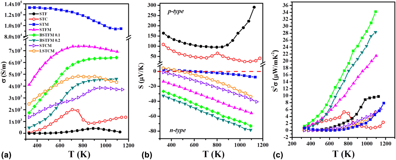
FIG. 8. TE properties: (a) electrical conductivity, (b) Seebeck coefficient, and (c) power factor of La and Ba doped STCM and STFM-based ceramics.
VIII. CHARGE TRANSPORT MECHANISM IN DOUBLE PEROVSKITES
In these types of transition metal-based perovskites, band model may not be a proper way to understand the conduction mechanism. In these materials, charge carriers are expected to be localized at defect sites. So activation energy should be required to overcome the energy barrier to delocalize these carriers resulting in effective charge transport in the double perovskite. To explain the conduction mechanism, small polaron hopping conduction seems more suitable for these systems.Reference Mott and Friedman83–Reference Tsuda, Nasu, Fujimori and Siratori85 Equation (19) expressed the small polaron hopping conduction mechanism.Reference Nag and Shubha86
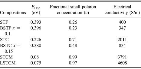
where E Hop is the activation energy of polarons, T is the temperature, and k B is the Boltzmann constant. If the small polaron hopping conduction is followed, then there should be a linear relation between ln (σT) and 1/k BT. Double perovskite oxides followed the small polaron hopping conduction mechanism in the semiconductor region of the conductivity curve as evident from the good linear fit shown in Fig. 9 for various double perovskite systems. Activation energy ‘E Hop’ is equal to the slope of the curve between ln (σT) and 1/k BT. Table III presents the calculated E Hop values for double perovskite oxides.
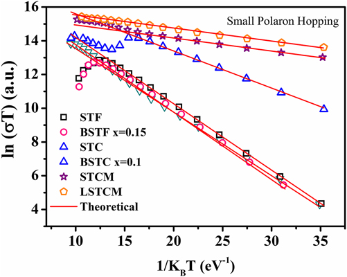
FIG. 9. Small polaron hopping (SPH) fitting of electrical conductivity of different double perovskite ceramic samples.
TABLE III. The calculated value of E Hop required for generation of the charge carrier.
Thermopower is fundamentally a transport entropy of charge carrier that discloses the further information regarding charge transport mechanism. For these perovskite oxides in which small polaron hopping model drives conduction mechanism, thermopower can be explained by Heikes formula. Chaikin and Beni modified the formula to address the spin interactions of the electron better as given by the following equationReference Chaikin and Beni87:
where ‘c’ is the fractional small polaron concentration arising from multivalent cations occupying similar lattice sites. Estimated values of c for double perovskite oxides are given in Table II. It is evident that as the activation energy decreases and the fractional polaron concentration, ‘c’ values increase in these double perovskites, the electrical conductivity of the material increases, which further validates the proposed model for charge transport mechanism in these double perovskites.
IX. COLOSSAL CHANGE IN THERMOPOWER
Understanding the relationships between the structural and chemical compatibility, solid solubility, thermal stability, and lattice strain in perovskite structure can help in developing a broad range of novel functional materials. In modern electronics, development of novel inorganic semiconductor-based p–n junction has become pivotal for application in switches,Reference Waser and Aono88 memory devices,Reference Chon, Jang, Kim and Chang89 transistors,Reference Mathews, Ramesh, Venkatesan and Benedetto90 sensorsReference Fergus91 etc.
In the current investigation, in the course of searching n-type oxide TE materials, we developed some novel SrTiO3-based double perovskites, such as BaxSr2−xTi0.8Fe0.8Nb0.4O6 (BSTFN), and LaxSr2−xTiFeO6 (LSTF) which exhibited metal–semiconductor transition induced p–n type conduction switching with colossal change in thermopower. These BSTFN and LSTF ceramics were synthesized by the solid-state method with different amounts of Ba and La in the Sr site of Sr2TiFeO6-based double perovskites. Both the compositions, BSTFN and LSTF, exhibited semiconductor (dσ/dT > 0) to metal-like (dσ/dT < 0) transition and temperature driven p–n type conduction switching with enormous change in thermopower, as shown in Fig. 10. Also, the variation of thermopower of these double perovskites is depicted in Table IV.
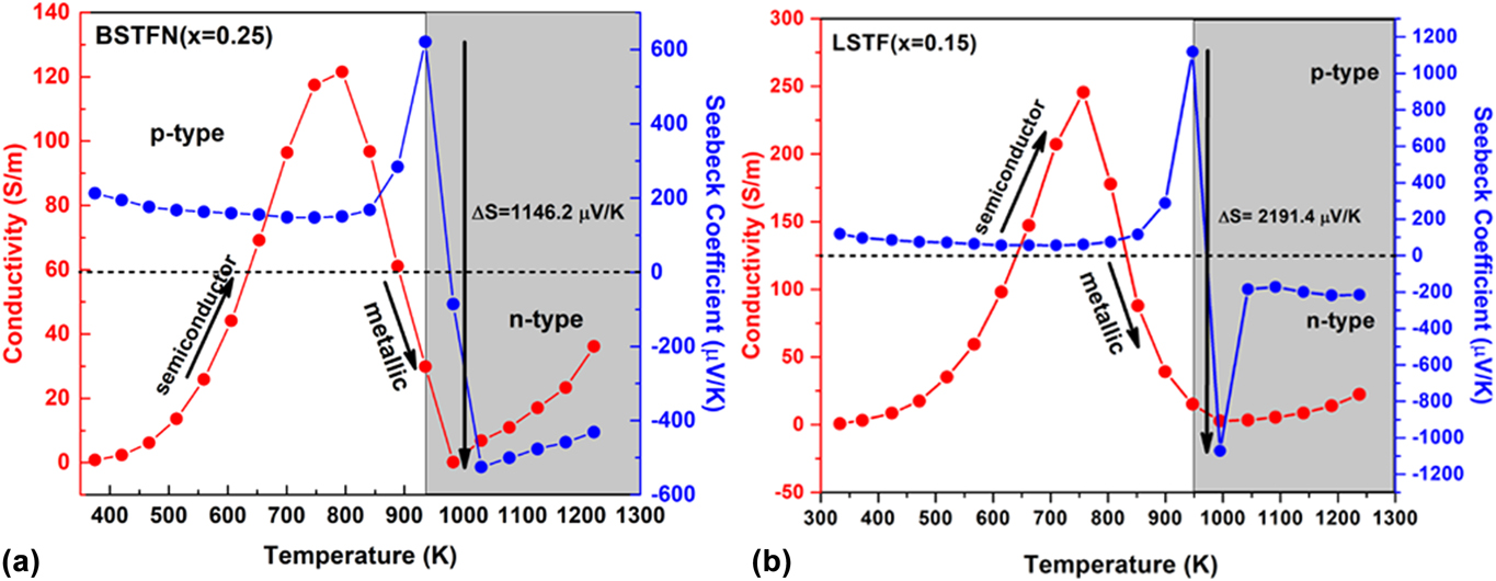
FIG. 10. The electrical conductivity and thermopower variation with temperature for (a) BSTFN (x = 025) and (b) LSTF (x = 0.15) double perovskites. Reproduced from Reference Roy, Waghmare, Tanwar and MaitiRef. 20 with permission from PCCP Owner Societies.
TABLE IV. Change in thermopower and its corresponding temperature obtained from the temperature-dependent thermopower graph for BSTFN and LSTF ceramics.

The conduction switching of these compositions was first tried to be understood by the source of charge carriers. The source of positive charge carriers in Sr2TiFeO6 (STF) was explained by defect reaction expressed by Eq. (10) using Kroger Vink notation, where the substitution of Ti4+ ion with Fe3+ gave rise to holes as majority charge carriers. The n-type behavior of the Sr2Ti0.8Fe0.8Nb0.4O6 (STFN) ceramics at higher temperature arose due to the doping of Nb5+ in the place of Ti4+ ion at the B-site of the double perovskite structure as expressed by Eq. (21), suggesting electrons as the charge carriers.
To verify the oxidation state of the B site cations, we further performed X-ray photoelectron spectroscopy of the BSTFN compositions and it confirms the presence of Fe in 3+ and 2+ states,Reference Yamashita and Hayes92,Reference Paparazzo93 Nb in 5+ and 4+ statesReference Lee, Kim, Yang and Choy94,Reference Carmalt, Manning, Parkin, Peters and Hector95 and Ti in 4+ & 3+ states,Reference Dementjev, Ivanova, Vasilyev, Naumkin, Nemirovsky and Shalaev96,Reference Lu, Kuang and Huang97 as shown in Figs. 11(a)–11(c), respectively.

FIG. 11. The respective binding energy of Fe, Nb, and Ti in BSTFN double perovskite obtained by X-ray photoelectron spectroscopy.
It is clear from the XPS analysis that pure STF, which behaved previously as a p-type semiconductor exhibited conduction switching (p to n-type) due to the incorporation of Nb in the B site of these double perovskite. Similarly, the n-type behavior of LSTF double perovskites can be described by Eqs. (13) and (15) and it is apparent that both electrons and holes are present in the BSTFN and LSTF systems. Hence the thermopower was compensated by both types of charge carriers resulting in low values of S at room temperature, where it does not produce much electrical conductivity. However, the holes contributed by defect reaction Eq. (10) act as the dominant source of charge carriers from room temperature up to T p–n, resulting in a positive thermopower value in the S versus T graph in both the ceramics, whereas beyond T p–n, Eqs. (13), (15), and (21) dominated the conductivity behavior of these samples. The dominant defect reactions determine the major carriers in the system. Nevertheless, in these double perovskite systems, a p-type-to-n-type semiconductor phase transformation occurred via an intermediate metallic phase. Hence, it was hypothesized that p–n-type switching facilitated large electron restructuring in LSTF and BSTFN, which was responsible for colossal change in thermopower. Further investigation to trap those structural changes in high temperature XRD is currently underway.
Previously such p–n type conduction switching assisted large change in thermopower was reported in the literature for few chalcogenide-based compounds, only in the last five years. But for the very first time it was observed in perovskite-based oxide materials and also the change in thermopower was larger than the previously reported results, as shown in the comparisonReference Roy, Waghmare, Tanwar and Maiti20,Reference Roy and Maiti21,Reference Guin, Pan, Bhowmik, Sanyal, Waghmare and Biswas98–Reference Osters, Bawohl, Bobet, Chevalier, Decourt and Nilges102 bar chart in Fig. 12. Such p–n switching coupled with a large change in thermopower in a single material as a result of only temperature change, opens up a new avenue for developing novel high-temperature diodes, thyristors, sensors, switches, thermistors, etc. The target areas for these devices are envisaged in space, chemical plants, automobile industries, and consumer electronics like cell phones, in which overheating or overcharging can cause the explosion of batteries due to thermal runaway. Colossal change in thermopower on the order of a few millivolts per Kelvin, integrated with p–n-type conduction switching, may lead to the development of novel thermal runaway monitors. Moreover, it can also be used for chemical-to-thermal-to-electrical energy conversion on the basis of the recently developed thermopower wave concept.

FIG. 12. Comparison of the maximum change in thermopower (ΔS) coupled with p–n type resistance switching behavior observed in different materials.
X. CONCLUSION
In the current work, a wide range of double perovskite oxide-based high-temperature TE materials were synthesized by the solid-state reaction method. The crystal structure of these materials was found to be cubic with ![]() $Pm\bar{3}m$ space group. A dense microstructure structure with grain size distribution scaling from nm to μm range was achieved in these double perovskites. It was shown that by manipulating cations and processing parameters, one can optimize electrical conductivity and Seebeck coefficient in these double perovskite oxides to achieve very good TE power factor. However, shift in semiconductor to metal transition temperature, TS-M by the doping played a key role in determining the operational temperature of these TE materials with maximum ZT values. Some of these double perovskites oxides also demonstrated temperature driven p–n switching assisted colossal change in Seebeck coefficient, which can be used for developing novel multifunctional devices. Conduction mechanism of these materials was explained by the small polaron hopping model. These double perovskites also showed low-temperature relaxor ferroelectric behavior inducing dipolar glassy phase. We demonstrated that using these relaxors above the Burns temperature, one can use the glassy phase of relaxor to obtain very low thermal conductivity without affecting its electrical conductivity. In other words, inducing glassy phase as a result of relaxor ferroelectricity in double perovskites can be a right approach for decoupling “Phonon-Glass Electron Crystal” behavior in these oxides. Nevertheless, ZT values of these oxides are lower compared to that of chalcogenides and intermetallics, although oxides showed good thermal stability at high temperature. More efforts are needed to improve the ZT values of these double perovskite oxides to realize the commercialization of these materials for TE power generation.
$Pm\bar{3}m$ space group. A dense microstructure structure with grain size distribution scaling from nm to μm range was achieved in these double perovskites. It was shown that by manipulating cations and processing parameters, one can optimize electrical conductivity and Seebeck coefficient in these double perovskite oxides to achieve very good TE power factor. However, shift in semiconductor to metal transition temperature, TS-M by the doping played a key role in determining the operational temperature of these TE materials with maximum ZT values. Some of these double perovskites oxides also demonstrated temperature driven p–n switching assisted colossal change in Seebeck coefficient, which can be used for developing novel multifunctional devices. Conduction mechanism of these materials was explained by the small polaron hopping model. These double perovskites also showed low-temperature relaxor ferroelectric behavior inducing dipolar glassy phase. We demonstrated that using these relaxors above the Burns temperature, one can use the glassy phase of relaxor to obtain very low thermal conductivity without affecting its electrical conductivity. In other words, inducing glassy phase as a result of relaxor ferroelectricity in double perovskites can be a right approach for decoupling “Phonon-Glass Electron Crystal” behavior in these oxides. Nevertheless, ZT values of these oxides are lower compared to that of chalcogenides and intermetallics, although oxides showed good thermal stability at high temperature. More efforts are needed to improve the ZT values of these double perovskite oxides to realize the commercialization of these materials for TE power generation.
ACKNOWLEDGMENT
This work is supported by the grant from Science and Engineering Research Board, DST (SERB-DST), India (Grant No. SB/S3/ME/008/2015).


