Article contents
In situ stress measurements during direct MOCVD growth of GaN on SiC
Published online by Cambridge University Press: 24 August 2015
Abstract

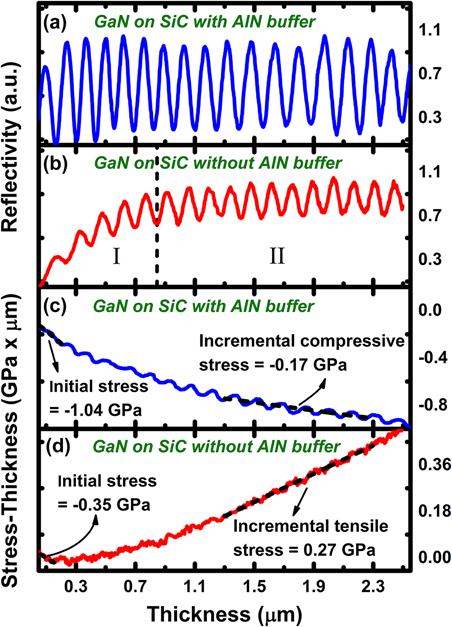
In situ curvature measurements were used to compare the stress evolution of GaN films grown directly on 6H-SiC via a two-step temperature growth to films grown with an AlN buffer layer. The two-step temperature growth consisted of an initial low-temperature and a main high-temperature GaN layer. In the case of GaN grown directly on 6H-SiC, the high-temperature layer initiated growth under compressive stress which transitioned to tensile stress. Films grown directly on 6H-SiC exhibited a reduction in the threading dislocation (TD) density and an improvement in the surface roughness compared to growth on the AlN buffer layer. Furthermore, transmission electron microscopy of the GaN grown directly on 6H-SiC revealed predominant (a + c)-type TD along with basal plane stacking faults and  $\left\{ {11\bar 20} \right\}$ prismatic stacking faults. Channeling cracks were observed in the GaN film when the AlN buffer layer was not utilized. This was attributed to tensile stress induced from the thermal expansion coefficient mismatch.
Keywords
- Type
- Articles
- Information
- Journal of Materials Research , Volume 30 , Issue 19: Focus Issue: Nitrides and Oxynitride Materials , 14 October 2015 , pp. 2900 - 2909
- Copyright
- Copyright © Materials Research Society 2015
References
REFERENCES
- 6
- Cited by


