Hostname: page-component-745bb68f8f-grxwn Total loading time: 0 Render date: 2025-01-14T19:09:12.520Z Has data issue: false hasContentIssue false

Kinetic study of the intermetallic compound formation between eutectic Sn–3.5Ag alloys and electroplated Ni metallization in flip-chip solder joints

Published online by Cambridge University Press:  28 February 2012

Hsiao-Yun Chen
Affiliation:
Department of Materials Science and Engineering, National Chiao Tung University, Hsinchu, Taiwan 30010, Republic of China
Chih Chen*
Affiliation:
Department of Materials Science and Engineering, National Chiao Tung University, Hsinchu, Taiwan 30010, Republic of China
*
a)Address all correspondence to this author. e-mail: chih@faculty.nctu.edu.tw
Get access

Abstract

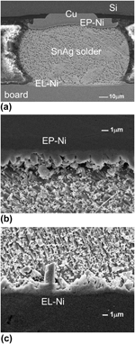
Ni-based under-bump metallization (UBM) has attracted wide attention due to its low reaction rate with Sn, compared with Cu and Cu alloy. In this study, the interfacial reactions between eutectic Sn–3.5Ag solder and Ni-based UBM, including electroplated Ni (EP-Ni) and electroless Ni (EL-Ni) are investigated. Morphology and growth kinetics of Ni3Sn4 intermetallic compounds are studied at different reflow temperatures and durations. The growth rate and the growth activation energy of Ni3Sn4 were measured for the two sets of samples. The activation energies are measured to be 25 kJ/mol and 38 kJ/mol for the Ni3Sn4 growth on EP-Ni and EL-Ni, respectively. The Ni3Sn4 on EP-Ni UBMs shows a slower growth rate and the Ni3Sn4/solder interface is void free even after 20-min reflow at 240 °C. On the other hand, the interface of Ni3Sn4/EL-Ni has a lot of microvoids after reflowing at 240 °C for 20 min.

Type
Articles
Copyright
Copyright © Materials Research Society 2012

Access options

Get access to the full version of this content by using one of the access options below. (Log in options will check for institutional or personal access. Content may require purchase if you do not have access.)

References

REFERENCES

1.Tu, K.N., Gusak, A.M., and Li, M.: Physics and materials challenges for lead-free solders. J. Appl. Phys. 93, 1335 (2003).CrossRefGoogle Scholar
2.Suraski, D. and Seelig, K.: The current status of lead-free solder alloys. IEEE Trans. Electron. Packag. Manuf. 24(4), 244 (2001).CrossRefGoogle Scholar
3.Zeng, K. and Tu, K.N.: Six cases of reliability study of Pb-free solder joints in electronic packaging technology. Mater. Sci. Eng., R 38, 55 (2002).CrossRefGoogle Scholar
4.Kang, S.K. and Ramachandran, V.: Growth kinetics of intermetallic phases at the liquid Sn and solid Ni interface. Scr. Mater. 14, 421 (1980).Google Scholar
5.Alam, M.O., Chan, Y.C., and Hung, K.C.: Interfacial reaction of Pb–Sn solder and Sn–Ag solder with electroless Ni deposit during reflow. J. Electron. Mater. 31, 1117 (2002).CrossRefGoogle Scholar
6.Yoon, J.W., Kim, S.W., and Jung, S.B.: Effect of reflow time on interfacial reaction and shear strength of Sn–0.7Cu solder/Cu and electroless Ni–P BGA joints. J. Alloy. Comp. 385, 192 (2004).CrossRefGoogle Scholar
7.Tu, K.N. and Zeng, K.: Tin–lead (SnPb) solder reaction in flip chip technology. Mater. Sci. Eng., R 34(1), 1 (2001).CrossRefGoogle Scholar
8.Kim, H.K. and Tu, K.N.: Rate of consumption of Cu in soldering accompanied by ripening. Appl. Phys. Lett. 67, 2002 (1995).CrossRefGoogle Scholar
9.Liu, A.A., Kim, K.N., and Totta, P.A.: Spalling of Cu6Sn5 spheroids in the soldering reaction of eutectic SnPb on Cr/Cu/Au thin films. J. Appl. Phys. 80, 2774 (1996).CrossRefGoogle Scholar
10.Kim, H.K., Tu, K.N., and Totta, P.A.: Ripening-assisted asymmetric spalling of Cu–Sn compound spheroids in solder joints on Si wafers. Appl. Phys. Lett. 68(16), 2204 (1996).CrossRefGoogle Scholar
11.Wassink, R.J.K.: Soldering in Electronics, 2nd ed. (Electrochemical Publications, United Kingdom, 1984).Google Scholar
12.Kim, P.G., Jang, J.W., Lee, T.Y., and Tu, K.N.: Interfacial reaction and wetting behavior in eutectic SnPb solder on Ni/Ti thin films and Ni foils. J. Appl. Phys. 86, 6746 (1999).CrossRefGoogle Scholar
13.Lin, K.L. and Liu, Y.C.: Reflow and property of Al/Cu/electroless nickel/Sn–Pb solder bumps. IEEE Trans. Adv. Packag. 22(4), 568 (1992).Google Scholar
14.Yoon, J.W. and Jung, S.B.: Growth kinetics of Ni3Sn4 and (NiP)-P-3 layer between Sn–3.5Ag solder and electroless Ni–P substrate. J. Alloy. Comp. 376, 105 (2004).CrossRefGoogle Scholar
15.Lee, C.Y. and Lin, K.L.: The interaction kinetics and compound formation between electroless Ni–P and solder. Thin Solid Films 249(2), 201 (1994).CrossRefGoogle Scholar
16.Jang, J.W., Kim, P.G., and Tu, K.N.: Solder reaction-assisted crystallization of electroless Ni–P under bump metallization in low cost flip chip technology. J. Appl. Phys. 85(12), 8456 (1999).CrossRefGoogle Scholar
17.Hung, K.C., Chen, Y.C., Tang, C.W., and Ong, H.C.: Correlation between Ni3Sn4 intermetallics and Ni3P due to solder reaction-assisted crystallization of electroless Ni–P metallization in advanced packages. J. Mater. Res. 15(11), 2534 (2000).CrossRefGoogle Scholar
18.Hung, K.C. and Chen, Y.C.: Study of Ni3P growth due to solder reaction-assisted crystallization of electroless Ni–P metallization. J. Mater. Sci. Lett. 19, 1755 (2000).CrossRefGoogle Scholar
19.Liu, P.L. and Shang, J.K.: A comparative fatigue study of solder/electroless-nickel and solder/copper interfaces. J. Mater. Res. 15(11), 2347 (2000).CrossRefGoogle Scholar
20.Peng, S.P., Andersson, C., and Wei, X.C.: High temperature aging study of intermetallic compound formation of Sn–3.5Ag and Sn–4.0Ag–0.5Cu solders on electroless Ni(P) metallization. J. Alloy. Comp. 452, 191 (2006).Google Scholar
21.Peng, S.P., Wu, W.H., Ho, C.E., and Huang, Y.M.: Comparative study between Sn37Pb and Sn3Ag0.5Cu soldering with Au/Pd/Ni(P) tri-layer structure. J. Alloy. Comp. 493, 431 (2009).CrossRefGoogle Scholar
22.Jang, J.W., Peter, D.R., Lee, T.Y., and Tu, K.N.: Morphology of interfacial reaction between lead-free solders and electroless Ni–P under bump metallization. J. Appl. Phys. 88, 6359 (2000).CrossRefGoogle Scholar
23.He, M., Lau, W.H., Qi, G., and Chen, Z.: Intermetallic compound formation between Sn–3.5Ag solder and Ni-based metallization during liquid state reaction. Thin Solid Films 462463, 376 (2004).CrossRefGoogle Scholar
24.Lin, Y.C., Shih, T.Y., Tien, S.K., and Duh, J.G.: Suppressing Ni–Sn–P growth in SnAgCu/Ni–P solder joints. Scr. Mater. 56, 49 (2007).CrossRefGoogle Scholar
25.Sharif, A., Chan, Y.C., Islam, M.N., and Rizvi, M.J.: Dissolution of electroless Ni metallization by lead-free solder alloys. J. Alloy. Comp. 388, 75 (2005).CrossRefGoogle Scholar
26.He, M., Kumar, A., Yeo, P.T., Qi, G.J., and Chen, Z.: Interfacial reaction between Sn-rich solders and Ni-based metallization. Thin Solid Films 462463, 387 (2004).CrossRefGoogle Scholar
27.Ghosh, G.: Coarsening kinetics of Ni3Sn4 scallops during interfacial reaction between liquid eutectic solders and Cu/Ni/Pd metallization. J. Appl. Phys. 88, 6887 (2000).CrossRefGoogle Scholar
28.Tu, P.L., Chan, Y.C., Hung, K.C., and Lai, J.K.L.: Effect of cooling rate on the isothermal fatigue behavior of CBGA solder joints in shear. Scr. Mater. 44, 317 (2001).CrossRefGoogle Scholar
29.Ghosh, G.: Dissolution and interfacial reactions of thin-film Ti/Ni/Ag metallizations in solder joints. Acta Mater. 49, 2609 (2001).CrossRefGoogle Scholar
30.Li, J.F., Mannan, S.H., Clode, M.P., Chen, K., Whalley, D.C., Liu, C., and Hutt, D.A.: Comparison of interfacial reactions of Ni and Ni–P in extended contact with liquid Sn–Bi-based solders. Acta Mater. 55, 737 (2007).CrossRefGoogle Scholar
31.Ghosh, G.: Interfacial microstructure and the kinetics of interfacial reaction in diffusion couples between Sn–Pb solder and Cu/Ni/Pd metallization. Acta Mater. 48, 3719 (2000).CrossRefGoogle Scholar
32.Shen, J., Chan, Y.C., and Liu, S.Y.: Growth mechanism of Ni3Sn4 in a Sn/Ni liquid/solid interfacial reaction. Acta Mater. 57, 5196 (2009).CrossRefGoogle Scholar
33.Lin, Y.C., Wang, K.J., and Duh, J.G.: Detailed phase evolution of phosphorous-rich layer and formation of Ni–Sn–P compound in SnAgCu/electroplated Ni–P solder joint. J. Electron. Mater. 39, 283 (2010).CrossRefGoogle Scholar
34.Takaku, Y., Liu, X.J., Ohnuma, I., Kainuma, R., and Ishida, K.: Interfacial reaction and morphology between molten Sn base solders and Cu substrate. Mater. Trans. 45, 646 (2004).CrossRefGoogle Scholar
35.Dauskardt, R.H., Haubensak, F., and Ritchie, R.O.: On the interpretation of the fractal character of fracture surfaces. Acta Mater. 38(2), 143 (1990).CrossRefGoogle Scholar
36.Kim, H.K. and Tu, K.N.: Kinetic analysis of the soldering reaction between eutectic SnPb alloy and Cu accompanied by ripening. Phys. Rev. B 53, 16027 (1996).CrossRefGoogle ScholarPubMed
37.Kang, S.K., Rai, R.S., and Purushothaman, S.: Interfacial reactions during soldering with lead–tin eutectic and lead (Pb)–free, tin-rich solders. J. Electron. Mater. 25, 1113 (1996).CrossRefGoogle Scholar
38.Gur, D. and Bamberger, M.: Reactive isothermal solidification in the Ni–Sn system. Acta Mater. 46, 4917 (1998).CrossRefGoogle Scholar
39.Jeon, Y.D., Paik, K.W., Bok, K.S., Choi, W.S., and Cho, C.L.: Studies of electroless nickel under bump metallurgy—Solder interfacial reactions and their effects on flip chip solder joint reliability. J. Electron. Mater. 31, 520 (2002).CrossRefGoogle Scholar
40.Chen, C.M. and Chen, S.W.: Electromigration effect upon the Sn–0.7 wt% Cu/Ni and Sn–3.5 wt% Ag/Ni interfacial reactions. J. Appl. Phys. 90(3), 1208 (2001).CrossRefGoogle Scholar
41.Ho, C.E., Yang, S.C., and Kao, C.R.: Interfacial reaction issues for lead-free electronic solders. J. Mater. Sci. Mater. Electron. 18, 155 (2007).CrossRefGoogle Scholar