Article contents
Comparison of Orientation Mapping in SEM and TEM
Published online by Cambridge University Press: 25 June 2020
Abstract

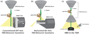
Multiple experimental configurations for performing nanoscale orientation mapping are compared to determine their fidelity to the true microstructure of a sample. Transmission Kikuchi diffraction (TKD) experiments in a scanning electron microscope (SEM) and nanobeam diffraction (NBD) experiments in a transmission electron microscope (TEM) were performed on thin electrodeposited hard Au films with two different microstructures. The Au samples either had a grain size that is >50 or <20 nm. The same regions of the samples were measured with TKD apparatuses at 30 kV in an SEM with detectors in the horizontal and vertical configurations and in the TEM at 300 kV. Under the proper conditions, we demonstrate that all three configurations can produce data of equivalent quality. Each method has strengths and challenges associated with its application and representation of the true microstructure. The conditions needed to obtain high-quality data for each acquisition method and the challenges associated with each are discussed.
Keywords
- Type
- Software and Instrumentation
- Information
- Copyright
- Copyright © Microscopy Society of America 2020
References
- 5
- Cited by


