Hostname: page-component-5f745c7db-sbzbt Total loading time: 0 Render date: 2025-01-06T12:33:22.161Z Has data issue: true hasContentIssue false

Contamination Mitigation Strategy for Ultra-Low Energy Electron Microscopy and Spectroscopy

Published online by Cambridge University Press:  05 August 2019

Eliška Materna Mikmeková*
Affiliation:
Department of Electron Microscopy, Institute of Scientific Instruments of the CAS, v. v. i., Brno, Czech Republic.
Luděk Frank
Affiliation:
Department of Electron Microscopy, Institute of Scientific Instruments of the CAS, v. v. i., Brno, Czech Republic.
Ivo Konvalina
Affiliation:
Department of Electron Microscopy, Institute of Scientific Instruments of the CAS, v. v. i., Brno, Czech Republic.
Ilona Müllerová
Affiliation:
Department of Electron Microscopy, Institute of Scientific Instruments of the CAS, v. v. i., Brno, Czech Republic.
Tao Zhang
Affiliation:
Department of Chemistry and Chemical Biology and Department of Chemical and Biochemical Engineering, Rutgers University, Piscataway NJ, USA.
Tewodros Asefa
Affiliation:
Department of Chemistry and Chemical Biology and Department of Chemical and Biochemical Engineering, Rutgers University, Piscataway NJ, USA.
*
*Corresponding author: eliska.mikmekova@isibrno.cz

Abstract

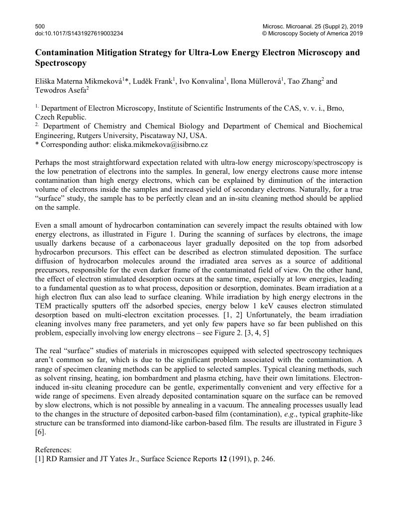
Image of the first page of this content. For PDF version, please use the ‘Save PDF’ preceeding this image.'
Type
Low Voltage, Low Energy Electron Microscopy Imaging and Analysis
Copyright
Copyright © Microscopy Society of America 2019 

References

[1]Ramsier, RD and Yates, JT Jr., Surface Science Reports 12 (1991), p. 246.Google Scholar
[2]Madye, TE and Yates, JT Jr., Journal of Vacuum Science and Technology 8 (1995), p. 525.Google Scholar
[3]Frank, L, Mikmeková, E and Lejeune, M, Applied Surface Science 407 (2017), p. 105.Google Scholar
[4]Mikmeková, E et al. , Diamond and Related Materials 63 (2015), p. 136.Google Scholar
[5]Suzuki, S in “Nanotechnology and Nanomaterials: Electronic Properties of Carbon Nanotubes”, (2011) p. 329.Google Scholar
[6]The authors acknowledge funding from the Technology Agency of the Czech Republic (Centre of Electron and Photonic Optics, no: TN01000008 and TG03010046).Google Scholar