Published online by Cambridge University Press: 23 November 2020

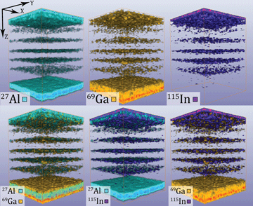
Atomic force microscopy (AFM) is a well-known tool for studying surface roughness and to collect depth information about features on the top atomic layers of samples. By combining secondary ion mass spectroscopy (SIMS) with focused ion beam (FIB) milling in a scanning electron microscope (SEM), chemical information of sputtered structures can be visualized and located with high lateral and depth resolution. In this paper, a high vacuum (HV) compatible AFM was installed in a TESCAN FIB-SEM instrument that was equipped with a time-of-flight SIMS (ToF-SIMS) detector. To calibrate the sputtering rate and measure the induced roughness caused by the ToF-SIMS analysis, subsequent AFM measurements were performed on an inorganic multilayer vertical cavity surface-emitting laser sample. Normalized sputtering rates were used to aid the accurate three-dimensional reconstruction of the sputtered volume's chemical composition. Achievable resolution, surface roughness during sputtering, and surface oxidation issues were analyzed. The integration of complementary detectors opens up the ability to determine the sample properties as well as to understand the influence of the Ga+ ion sputtering method on the sample surface during the analysis.