Hostname: page-component-745bb68f8f-v2bm5 Total loading time: 0 Render date: 2025-01-07T21:45:17.275Z Has data issue: false hasContentIssue false

TEM Imaging of Edges and Point Defects in Monolayer Phosphorene

Published online by Cambridge University Press:  30 July 2020

Yangjin Lee
Affiliation:
Yonsei University, Seoul, Seoul-t'ukpyolsi, Republic of Korea
Sol Lee
Affiliation:
Yonsei University, Seoul, Seoul-t'ukpyolsi, Republic of Korea
Jun-Yeong Yoon
Affiliation:
Yonsei University, Seoul, Seoul-t'ukpyolsi, Republic of Korea
Jinwoo Cheon
Affiliation:
Yonsei University, Seoul, Seoul-t'ukpyolsi, Republic of Korea
Hu Young Jeong
Affiliation:
Ulsan National Institute of Science and Technology (UNIST), Ulsan, Ulsan-gwangyoksi, Republic of Korea
Kwanpyo Kim
Affiliation:
Yonsei University, Seoul, Seoul-t'ukpyolsi, Republic of Korea

Abstract

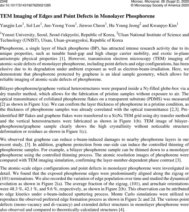
Image of the first page of this content. For PDF version, please use the ‘Save PDF’ preceeding this image.'
Type
New Frontiers in Electron Microscopy of Two-dimensional Materials
Copyright
Copyright © Microscopy Society of America 2020

References

Ling, X., et al. ., Proc. Natl. Acad. Sci. U. S. A. 112 (2015) 4523.10.1073/pnas.1416581112CrossRefGoogle Scholar
Lee, Y., et al. , J Phys. D. J. Phys. D: Appl. Phys. 50 (2017) 084003.10.1088/1361-6463/aa5583CrossRefGoogle Scholar
Lee, Y. et al. ., Nano Lett. 20 (2020) 559-566.10.1021/acs.nanolett.9b04292CrossRefGoogle Scholar
The authors acknowledge funding from the Basic Science Research Program through the National Research Foundation of Korea (NRF) funded by the Ministry of Education (NRF-2017R1A5A1014862, NRF-2018R1A2B6008104) and the Institute for Basic Science (IBS-R026-D1).Google Scholar