Hostname: page-component-cd9895bd7-jkksz Total loading time: 0 Render date: 2024-12-27T08:35:09.237Z Has data issue: false hasContentIssue false

A Three-Dimensional Reconstruction Algorithm for Scanning Transmission Electron Microscopy Data from a Single Sample Orientation

Published online by Cambridge University Press:  24 June 2022
Hamish G. Brown*
Affiliation:
National Center for Electron Microscopy Facility, Molecular Foundry, Lawrence Berkeley National Laboratory, Berkeley, CA 94720, USA
Philipp M. Pelz
Affiliation:
National Center for Electron Microscopy Facility, Molecular Foundry, Lawrence Berkeley National Laboratory, Berkeley, CA 94720, USA Department of Materials Science and Engineering, University of California, Berkeley, CA 94720, USA
Shang-Lin Hsu
Affiliation:
National Center for Electron Microscopy Facility, Molecular Foundry, Lawrence Berkeley National Laboratory, Berkeley, CA 94720, USA Department of Materials Science and Engineering, University of California, Berkeley, CA 94720, USA
Zimeng Zhang
Affiliation:
Department of Materials Science and Engineering, University of California, Berkeley, CA 94720, USA
Ramamoorthy Ramesh
Affiliation:
Department of Materials Science and Engineering, University of California, Berkeley, CA 94720, USA Department of Physics, University of California, Berkeley, CA 94720, USA
Katherine Inzani
Affiliation:
Materials Sciences Division, Lawrence Berkeley National Laboratory, Berkeley, CA 94720, USA Molecular Foundry, Lawrence Berkeley National Laboratory, Berkeley, CA 94720, USA
Evan Sheridan
Affiliation:
Materials Sciences Division, Lawrence Berkeley National Laboratory, Berkeley, CA 94720, USA Molecular Foundry, Lawrence Berkeley National Laboratory, Berkeley, CA 94720, USA Theory and Simulation of Condensed Matter, Department of Physics, King's College London, The Strand, London WC2R 2LS, UK
Sinéad M. Griffin
Affiliation:
Materials Sciences Division, Lawrence Berkeley National Laboratory, Berkeley, CA 94720, USA Molecular Foundry, Lawrence Berkeley National Laboratory, Berkeley, CA 94720, USA
Marcel Schloz
Affiliation:
Department of Physics & IRIS Adlershof, Humboldt-Universität zu Berlin, Newtonstraße 15, 12489 Berlin, Germany
Thomas C. Pekin
Affiliation:
Department of Physics & IRIS Adlershof, Humboldt-Universität zu Berlin, Newtonstraße 15, 12489 Berlin, Germany
Christoph T. Koch
Affiliation:
Department of Physics & IRIS Adlershof, Humboldt-Universität zu Berlin, Newtonstraße 15, 12489 Berlin, Germany
Scott D. Findlay
Affiliation:
School of Physics and Astronomy, Monash University, Clayton, VIC 3800, Australia
Leslie J. Allen
Affiliation:
School of Physics, University of Melbourne, Parkville, VIC 3010, Australia
Mary C. Scott
Affiliation:
National Center for Electron Microscopy Facility, Molecular Foundry, Lawrence Berkeley National Laboratory, Berkeley, CA 94720, USA Department of Materials Science and Engineering, University of California, Berkeley, CA 94720, USA
Colin Ophus
Affiliation:
National Center for Electron Microscopy Facility, Molecular Foundry, Lawrence Berkeley National Laboratory, Berkeley, CA 94720, USA
Jim Ciston*
Affiliation:
National Center for Electron Microscopy Facility, Molecular Foundry, Lawrence Berkeley National Laboratory, Berkeley, CA 94720, USA
*
*Corresponding author: Hamish G. Brown, E-mail: hgbrown@unimelb.edu.au; Jim Ciston, E-mail: JCiston@lbl.gov
Get access

Abstract

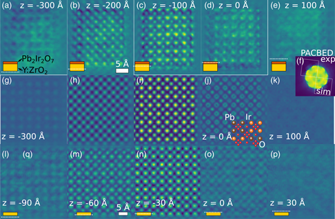
Increasing interest in three-dimensional nanostructures adds impetus to electron microscopy techniques capable of imaging at or below the nanoscale in three dimensions. We present a reconstruction algorithm that takes as input a focal series of four-dimensional scanning transmission electron microscopy (4D-STEM) data. We apply the approach to a lead iridate, Pb$_2$Ir$_2$O$_7$, and yttrium-stabilized zirconia, Y$_{0.095}$Zr$_{0.905}$O$_2$, heterostructure from data acquired with the specimen in a single plan-view orientation, with the epitaxial layers stacked along the beam direction. We demonstrate that Pb–Ir atomic columns are visible in the uppermost layers of the reconstructed volume. We compare this approach to the alternative techniques of depth sectioning using differential phase contrast scanning transmission electron microscopy (DPC-STEM) and multislice ptychographic reconstruction.

Type
Software and Instrumentation
Copyright
Copyright © The Author(s), 2022. Published by Cambridge University Press on behalf of the Microscopy Society of America

Access options

Get access to the full version of this content by using one of the access options below. (Log in options will check for institutional or personal access. Content may require purchase if you do not have access.)

Footnotes

Current address: Ian Holmes Imaging Centre, Bio21 Molecular Science and Biotechnology Institute, the University of Melbourne, Parkville, VIC 3052, Australia.

References

Allen, LJ, Faulkner, HML & Leeb, H (2000). Inversion of dynamical electron diffraction data including absorption. Acta Crystallogr A 56, 119126.CrossRefGoogle ScholarPubMed
Bosch, EGT & Lazić, I (2019). Analysis of depth-sectioning STEM for thick samples and 3D imaging. Ultramicroscopy 207, 112831.CrossRefGoogle ScholarPubMed
Brown, HG, Chen, Z, Weyland, M, Ophus, C, Ciston, J, Allen, LJ & Findlay, SD (2018). Structure retrieval at atomic resolution in the presence of multiple scattering of the electron probe. Phys Rev Lett 121, 266102.CrossRefGoogle ScholarPubMed
Chen, Z, Jiang, Y, Shao, YT, Holtz, ME, Odstrčil, M, Guizar-Sicairos, M, Hanke, I, Ganschow, S, Schlom, DG & Muller, DA (2021). Electron ptychography achieves atomic-resolution limits set by lattice vibrations. Science 372, 826831.CrossRefGoogle ScholarPubMed
Chen, Z, Weyland, M, Ercius, P, Ciston, J, Zheng, C, Fuhrer, MS, D'Alfonso, AJ, Allen, LJ & Findlay, SD (2016). Practical aspects of diffractive imaging using an atomic-scale coherent electron probe. Ultramicroscopy 169, 107121.CrossRefGoogle ScholarPubMed
Ciston, J, Deng, B, Marks, LD, Own, CS & Sinkler, W (2008). A quantitative analysis of the cone-angle dependence in precession electron diffraction. Ultramicroscopy 108, 514522.CrossRefGoogle ScholarPubMed
Close, R, Chen, Z, Shibata, N & Findlay, SD (2015). Towards quantitative, atomic-resolution reconstruction of the electrostatic potential via differential phase contrast using electrons. Ultramicroscopy 159, 124137.CrossRefGoogle ScholarPubMed
Coene, W & Van Dyck, D (1990). Inelastic scattering of high-energy electrons in real space. Ultramicroscopy 33, 261267.CrossRefGoogle Scholar
Cowley, JM & Moodie, AF (1957). Fourier images: II-The out-of-focus patterns. Proc Phys Soc B 70, 497.CrossRefGoogle Scholar
Donatelli, JJ & Spence, JCH (2020). Inversion of many-beam Bragg intensities for phasing by iterated projections: Removal of multiple scattering artifacts from diffraction data. Phys Rev Lett 125, 065502.CrossRefGoogle ScholarPubMed
Findlay, SD (2005). Quantitative structure retrieval using scanning transmission electron microscopy. Acta Crystallogr A 61, 397404.CrossRefGoogle ScholarPubMed
Gao, S, Wang, P, Zhang, F, Martinez, GT, Nellist, PD, Pan, X & Kirkland, AI (2017). Electron ptychographic microscopy for three-dimensional imaging. Nat Commun 8, 18.CrossRefGoogle ScholarPubMed
Guizar-Sicairos, M & Fienup, JR (2008). Phase retrieval with transverse translation diversity: A nonlinear optimization approach. Opt Express 16, 72647278.CrossRefGoogle ScholarPubMed
Jiang, Y, Chen, Z, El Baggari, I, Kourkoutis, LF, Elser, V & Muller, DA (2018 a). Breaking the Rayleigh limit in thick samples with multi-slice ptychography. Microsc Microanal 24, 192193.CrossRefGoogle Scholar
Jiang, Y, Chen, Z, Han, Y, Deb, P, Gao, H, Xie, S, Purohit, P, Tate, MW, Park, J, Gruner, SM, Elser, V & Muller, DA (2018 b). Electron ptychography of 2D materials to deep sub-ångström resolution. Nature 559, 343349.CrossRefGoogle Scholar
LeBeau, JM, Findlay, SD, Allen, LJ & Stemmer, S (2010). Position averaged convergent beam electron diffraction: Theory and applications. Ultramicroscopy 110, 118125.CrossRefGoogle ScholarPubMed
Maiden, AM, Humphry, MJ & Rodenburg, JM (2012). Ptychographic transmission microscopy in three dimensions using a multi-slice approach. JOSA A 29, 16061614.CrossRefGoogle ScholarPubMed
Nellist, PD, McCallum, BC & Rodenburg, JM (1995). Resolution beyond the ‘information limit’ in transmission electron microscopy. Nature 374, 630632.CrossRefGoogle Scholar
Nord, M, Vullum, PE, MacLaren, I, Tybell, T & Holmestad, R (2017). Atomap: A new software tool for the automated analysis of atomic resolution images using two-dimensional Gaussian fitting. Adv Struct Chem Imaging 3, 9.CrossRefGoogle ScholarPubMed
Oh, MH, Cho, MG, Chung, DY, Park, I, Kwon, YP, Ophus, C, Kim, D, Kim, MG, Jeong, B, Gu, XW, Jo, J, Yoo, JM, Hong, J, McMains, S, Kang, K, Sung, Y-E, Alivisatos, AP & Hyeon, T (2020). Design and synthesis of multigrain nanocrystals via geometric misfit strain. Nature 577, 359363.CrossRefGoogle ScholarPubMed
Ophus, C (2019). Four-dimensional scanning transmission electron microscopy (4D-STEM): From scanning nanodiffraction to ptychography and beyond. Microsc Microanal 25, 563582.CrossRefGoogle ScholarPubMed
Ophus, C, Harvey, TR, Yasin, FS, Brown, HG, Pelz, PM, Savitzky, BH, Ciston, J & McMorran, BJ (2019). Advanced phase reconstruction methods enabled by four-dimensional scanning transmission electron microscopy. Microsc Microanal 25, 1011.CrossRefGoogle Scholar
Pelz, PM, Brown, HG, Stonemeyer, S, Findlay, SD, Zettl, A, Ercius, P, Zhang, Y, Ciston, J, Scott, MC & Ophus, C (2021). Phase-contrast imaging of multiply-scattering extended objects at atomic resolution by reconstruction of the scattering matrix. Phys Rev Res 3, 023159.CrossRefGoogle Scholar
Pennycook, TJ, Lupini, AR, Yang, H, Murfitt, MF, Jones, L & Nellist, PD (2015). Efficient phase contrast imaging in STEM using a pixelated detector. Part 1: Experimental demonstration at atomic resolution. Ultramicroscopy 151, 160167.CrossRefGoogle ScholarPubMed
Rodenburg, JM, McCallum, BC & Nellist, PD (1993). Experimental tests on double-resolution coherent imaging via STEM. Ultramicroscopy 48, 304314.CrossRefGoogle Scholar
Schloz, M, Pekin, TC, Chen, Z, den Broek, WV, Muller, DA & Koch, CT (2020). Overcoming information reduced data and experimentally uncertain parameters in ptychography with regularized optimization. Opt Express 28, 2830628323.CrossRefGoogle ScholarPubMed
Shibata, N, Kohno, Y, Findlay, SD, Sawada, H, Kondo, Y & Ikuhara, Y (2010). New area detector for atomic-resolution scanning transmission electron microscopy. J Electron Microsc (Tokyo) 59, 473479.CrossRefGoogle ScholarPubMed
Shibata, N, Seki, T, Sánchez-Santolino, G, Findlay, SD, Kohno, Y, Matsumoto, T, Ishikawa, R & Ikuhara, Y (2017). Electric field imaging of single atoms. Nat Commun 8, 17.CrossRefGoogle ScholarPubMed
Spence, JCH (1998). Direct inversion of dynamical electron diffraction patterns to structure factors. Acta Crystallogr A 54, 718.CrossRefGoogle Scholar
Sturkey, L (1962). The calculation of electron diffraction intensities. Proc Phys Soc 80, 321.CrossRefGoogle Scholar
Subramanian, M, Aravamudan, G & Subba Rao, G (1983). Oxide pyrochlores: A review. Prog Solid State Chem 15, 55143.CrossRefGoogle Scholar
Thibault, P & Guizar-Sicairos, M (2012). Maximum-likelihood refinement for coherent diffractive imaging. New J Phys 14, 063004.CrossRefGoogle Scholar
van Benthem, K, Lupini, AR, Oxley, MP, Findlay, SD, Allen, LJ & Pennycook, SJ (2006). Three-dimensional ADF imaging of individual atoms by through-focal series scanning transmission electron microscopy. Ultramicroscopy 106, 10621068.CrossRefGoogle ScholarPubMed
Wang, G, Giannakis, GB & Eldar, YC (2017). Solving systems of random quadratic equations via truncated amplitude flow. IEEE Trans Inf Theory 64, 773794.CrossRefGoogle Scholar
Weinberg, S (1995). The Quantum Theory of Fields, vol. 2. Cambridge, UK: Cambridge University Press.CrossRefGoogle Scholar
Withers, F, Del Pozo-Zamudio, O, Mishchenko, A, Rooney, AP, Gholinia, A, Watanabe, K, Taniguchi, T, Haigh, SJ, Geim, A, Tartakovskii, AI & Novoselov, KS (2015). Light-emitting diodes by band-structure engineering in van der Waals heterostructures. Nat Mater 14, 301306.CrossRefGoogle ScholarPubMed
Xin, HL & Muller, DA (2009). Aberration-corrected ADF-STEM depth sectioning and prospects for reliable 3D imaging in S/TEM. J Electron Microsc (Tokyo) 58, 157165.CrossRefGoogle ScholarPubMed
Yadav, A, Nelson, C, Hsu, S, Hong, Z, Clarkson, J, Schlepütz, C, Damodaran, A, Shafer, P, Arenholz, E, Dedon, L, Chen, D, Vishwanath, A, Minor, AM, Chen, LQ, Scott, JF, Martin, LW & Ramesh, R (2016). Observation of polar vortices in oxide superlattices. Nature 530, 198201.CrossRefGoogle ScholarPubMed
Yang, H, MacLaren, I, Jones, L, Martinez, GT, Simson, M, Huth, M, Ryll, H, Soltau, H, Sagawa, R, Kondo, Y, Ophus, C, Ercius, P, Jin, L, Kovács, A & Nellist, PD (2017 a). Electron ptychographic phase imaging of light elements in crystalline materials using Wigner distribution deconvolution. Ultramicroscopy 180, 173179.CrossRefGoogle ScholarPubMed
Yang, H, Rutte, R, Jones, L, Simson, M, Sagawa, R, Ryll, H, Huth, M, Pennycook, T, Green, M, Soltau, H, Kondo, Y, David, BG & Nellist, PD (2016). Simultaneous atomic-resolution electron ptychography and Z-contrast imaging of light and heavy elements in complex nanostructures. Nat Commun 7, 18.CrossRefGoogle ScholarPubMed
Yang, Y, Chen, CC, Scott, M, Ophus, C, Xu, R, Pryor, A, Wu, L, Sun, F, Theis, W, Zhou, J, Eisenbach, M, Kent, PRC, Sabirianov, RF, Zeng, H, Ercius, P & Miao, J (2017 b). Deciphering chemical order/disorder and material properties at the single-atom level. Nature 542, 7579.CrossRefGoogle ScholarPubMed
Supplementary material: File

Brown et al. supplementary material

Brown et al. supplementary material 1

Download Brown et al. supplementary material(File)
File 473.7 KB
Supplementary material: PDF

Brown et al. supplementary material

Brown et al. supplementary material 2

Download Brown et al. supplementary material(PDF)
PDF 5.6 MB