1 Introduction
Inertial fusion energy (IFE) requires semiconductor laser diode production and system integration on a large scale. Laser fusion research is carried out at research centres worldwide using single-shot high-energy lasers. Installations such as NIF, LMJ, LFEX, Shenguang-III and UFL-2m use flash lamp-pumped solid-state lasers[Reference Danson, Hillier, Hopps and Neely1]. For the construction of a power plant, the laser needs to operate repetitively, and the total power output directly depends on the laser’s electro-optical efficiency. The power plant scenarios LIFE[Reference Bayramian, Aceves, Anklam, Baker, Bliss, Boley, Bullington, Caird, Chen, Deri, Dunne, Erlandson, Flowers, Henesian, Latkowski, Manes, Molander, Moses, Piggott, Powers, Rana, Rodriguez, Sawicki, Schaffers, Seppala, Spaeth, Sutton and Telford2] and HiPER[Reference Chanteloup, Lucianetti, Albach and Novo3] estimate the laser pulse frequency between 10 and 16 Hz. These scenarios rely on different ignition schemes and diode-pumped solid-state laser (DPSSL) technologies. Until laser ignition is shown, these two studies represent the best estimates for the requirements of an IFE power plant on the DPSSL systems. The data are compared in Table 1 to the
Table 1. Inertial fusion laser requirements on pump diodes.
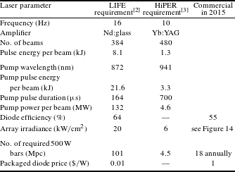
current state of the art in the laser diode industry. For the HiPER estimate, it must be noted that second or third harmonic generation are not accounted for and would, if required, raise the required pump pulse energies. Laser diodes are routinely used for pumping Nd:glass and Yb:YAG gain media at around 880 and 940 nm, respectively. The electro-optical efficiency of current series production 880 nm laser diodes is 55%, approaching the value assumed in the LIFE design. The array irradiance is a matter of the diode packaging density, and the requirements can be met as will be discussed below. An obvious mismatch between the LIFE requirement and commercial reality today lies in the availability and price of the laser bars. The need for 100 million chips for the construction of one power plant is contrasted by today’s annual production capacity, which we estimate at 18 million bars, the resources of all manufacturers and for all high-power semiconductor laser products combined. The price target formulated in the LIFE study is even two orders of magnitude below the current value. All of these values are very uncertain, but illustrate the challenges that the industry must face for IFE to become reality. In the following sections, we discuss how the issues of production capacity, laser diode efficiency and array irradiance can be addressed. We start with the existing proofs of concept.
2 Diode-pumped high-energy-class lasers installations
To date, high-energy-class-DPSSL (HEC-DPSSL) systems with the ignition pulse energy assumed in the LIFE and HiPER studies have been designed. Scalable engineering solutions have been tried, and laser systems delivering pulse energies of a hundredth of the requirement for one beam, such as DiPOLE[Reference Banerjee, Ertel, Mason, Phillips, Greenhalgh and Collier4], have been built. Systems expected to deliver a tenth of one beam’s pulse energy are currently being assembled, e.g., HiLASE L2[Reference Lucianetti, Divoky, Sawicka, Sikocinski, Jambunathan, Pilar, Slezak, Kmetik, Novak, Fibrich, Rus, Koerner, Hein and Mocek5] or ELI Beamlines L3[Reference Rus, Bakule, Kramer, Korn, Green, Nóvak, Fibrich, Batysta, Thoma, Naylon, Mazanec, Vítek, Barros, Koutris, Hr̈ebíc̈ek, Polan, Bas̈e, Homer, Kos̈elja, Havlíc̈ek, Honsa, Novák, Zervos, Korous, Laub and Houz̈vic̈ka6, Reference Thiagarajan, Smith, Helmrich, Pennington, Lohrenz, Cao, Ai, Walker and McElhinney7]. The pulse energy and repetition rates of these systems are a good measure of complexity of the laser installation, and are given in Figure 1. Balancing the availability of the gain crystals, the complexity of the temperature control and the trade-off between storage time and pump efficiency, different gain media have been chosen for these systems[Reference Erlandson, Aceves, Bayramian, Bullington, Beach, Boley, Caird, Deri, Dunne, Flowers, Henesian, Manes, Moses, Rana, Schaffers, Spaeth, Stolz and Telford8], and hence they are grouped by pump wavelength in Figure 1. Laser diodes emitting at 808 nm with 100 W per laser bar are used by KURE-I[Reference Matsumoto, Yasuhara, Kurita, Ikegawa, Sekine, Kawashima, Kawanaka, Norimatsu, Miyanaga, Izawa, Nakatsuka, Miyamoto, Kan, Furukawa and Motokoshi9]. Regarding the projects driven by 880 nm pump sources, Figure 1 shows that the GOLD[Reference Bayramian, Campbell, Ebbers, Freitas, Latkowski, Molander, Sutton, Telford and Caird10] and ELI beamlines L3 projects are designed to work more than an order of magnitude below the pump pulse energy and the average power estimated for LIFE. In the group of 9xx nm-pumped systems[Reference Chanteloup, Yu, Bourdet, Dambrine, Ferre, Fulop, Le Moal, Pichot, Le Touze and Zhao11, Reference Bayramian, Armstrong, Ault, Beach, Bibeau, Caird, Campbell, Chai, Dawson, Ebbers, Erlandson, Fei, Freitas, Kent, Liao, Ladran, Menapace, Molander, Payne, Peterson, Randles, Schaffers, Sutton, Tassano, Telford and Utterback12], the previous generation of Jenoptik’s 300 W bars was successfully used in the Polaris[Reference Hein, Kaluza, Bödefeld, Siebold, Podleska and Sauerbrey13] and DiPOLE[Reference Banerjee, Ertel, Mason, Phillips, Greenhalgh and Collier4] projects. Systems currently under construction with other suppliers include PEnELOPE[Reference Albach, Löser, Siebold and Schramm14] and HiLASE L2[Reference Lucianetti, Divoky, Sawicka, Sikocinski, Jambunathan, Pilar, Slezak, Kmetik, Novak, Fibrich, Rus, Koerner, Hein and Mocek5], marking a step ahead towards the estimated HiPER requirement. The pulse repetition rates given in Figure 1 are typically not limited by the pump diode technology, as will be shown below. Instead, it has been a concern of pump diode development to raise the output power of individual laser diode chips. Progress in semiconductor laser technology allows to increase the power per bar to 500 W now on a production scale, as will be discussed below. This will permit another step up in pump power without increasing the size of the optics.

Figure 1. Pump diode pulse energy levels of HEC-DPSSL installations, sorted by pump wavelength. Solid symbols: systems proven or under construction. Empty symbols: systems at design level.
3 Laser diode bars
The maximum optical power density of a laser bar is limited by the stability of the facets and the waste heat generation, which in turn leads to thermal rollover and degradation of the active region[Reference Pietrzak15]. For any given active region design, the output power per chip therefore scales almost linearly with the resonator length. This linear trend is apparent for continuous-wave (CW) operation diodes, as shown in Figure 2 for current 940 nm laser bars. The pulse length for pump diodes in pulsed lasers is close to the storage time of the gain media (Table 1). In this quasi-continuous wave (QCW) operation mode, the carrier and light distributions inside the semiconductor reach steady state, but thermal equilibrium is not reached. Simply speaking, the laser diode is turned off in every pulse before it runs hot. Therefore, the peak light output power in QCW operation is typically much higher for a chip of given geometry than what would be sustainable in CW operation. Figure 2 shows that this increase from CW power to QCW power amounts to more than a factor of three for laser bars with 1.5 mm resonator length. Nevertheless, an increase in QCW output power per chip area is only possible by the introduction of new designs for the active region. The Jenoptik’s New Generation (NG) epitaxial design together with the facet passivation thus raises the limit from 300 to 500 W per bar. An overview of high-power QCW laser bar specifications available now from Jenoptik is given in Table 2. We now describe the development of these devices briefly.

Figure 2. Illustration of Jenoptik’s 940 nm laser diode bar portfolio. For a given technology, the output power is linear with chip size. The New Generation (NG) QCW bars increase output power from 300 to 500 W at the fixed resonator length of 1.5 mm.

Figure 3. 808 nm QCW laser diode: output power-versus-current characteristic and efficiency.
3.1 808 nm QCW bars
The facet passivation introduced on all 500 W QCW bars permits to extend the operating range of the 808 nm QCW bar from 300 to 500 W. The new bars use a 37 emitter layout with 75% filling factor and 1.5 mm resonator length. The electro-optical characteristic is shown in Figure 3. A conversion efficiency of 52% is obtained at the operating point of 500 W. The laser diode exhibits a spectral width of 3.6 nm at half max., and 6.6 nm at 95% power content. Life testing of these bars is performed on microchannel heatsinks in pulsed operation. The pulse length ![]() ${\it\tau}$ is
${\it\tau}$ is ![]() $300~{\rm\mu}\text{s}$, the frequency
$300~{\rm\mu}\text{s}$, the frequency ![]() $f$ is 100 Hz, the coolant temperature
$f$ is 100 Hz, the coolant temperature ![]() $T_{c}$ is
$T_{c}$ is ![]() $25\,^{\circ }\text{C}$. The test is ongoing and has currently reached 700 Mshots without degradation of optical output power, as shown in Figure 4.
$25\,^{\circ }\text{C}$. The test is ongoing and has currently reached 700 Mshots without degradation of optical output power, as shown in Figure 4.

Figure 4. Life testing of 808 nm 500 W QCW bar in constant current mode. The bars are mounted on microchannel heatsinks with ![]() $T_{c}=25\,^{\circ }\text{C}$,
$T_{c}=25\,^{\circ }\text{C}$, ![]() ${\it\tau}=300~{\rm\mu}\text{s}$,
${\it\tau}=300~{\rm\mu}\text{s}$, ![]() $f=100$ Hz.
$f=100$ Hz.
Table 2. Jenoptik QCW laser diode bar specifications. All devices possess 37 emitters with a fill factor of 75%.
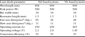
a 95% power content.
3.2 880 nm QCW bars
The new generation 880 nm QCW bar benefits from a good carrier confinement, resulting in a high gain, and a high slope efficiency[Reference Pietrzak, Hülsewede, Zorn, Hirsekorn, Sebastian, Meusel, Blümel and Hennig16]. The device is also passivated and has 37 emitters with 75% filling factor, and operates at 500 W at high efficiency with only 1.5 mm resonator length. The electro-optical data is shown by the characteristic in Figure 5, measured at ![]() ${\it\tau}=300~{\rm\mu}\text{s}$,
${\it\tau}=300~{\rm\mu}\text{s}$, ![]() $T_{c}=25\,^{\circ }\text{C}$. The spectral width under these conditions is 5.9 nm at 95% power content. The lateral emitter layout is optimized for optical mode confinement and generates a divergence as summarized in Table 2. The 880 nm bars are qualified for a useful lifetime of 1 Gshots. The reliability was proven on microchannel heatsinks in a life test running at 100 Hz, indicating no degradation in output power or change in emission wavelength, as can be seen in Figure 6[Reference Pietrzak, Hülsewede, Zorn, Hirsekorn, Meusel, Kindsvater, Schröder, Blümel and Sebastian17].
$T_{c}=25\,^{\circ }\text{C}$. The spectral width under these conditions is 5.9 nm at 95% power content. The lateral emitter layout is optimized for optical mode confinement and generates a divergence as summarized in Table 2. The 880 nm bars are qualified for a useful lifetime of 1 Gshots. The reliability was proven on microchannel heatsinks in a life test running at 100 Hz, indicating no degradation in output power or change in emission wavelength, as can be seen in Figure 6[Reference Pietrzak, Hülsewede, Zorn, Hirsekorn, Meusel, Kindsvater, Schröder, Blümel and Sebastian17].
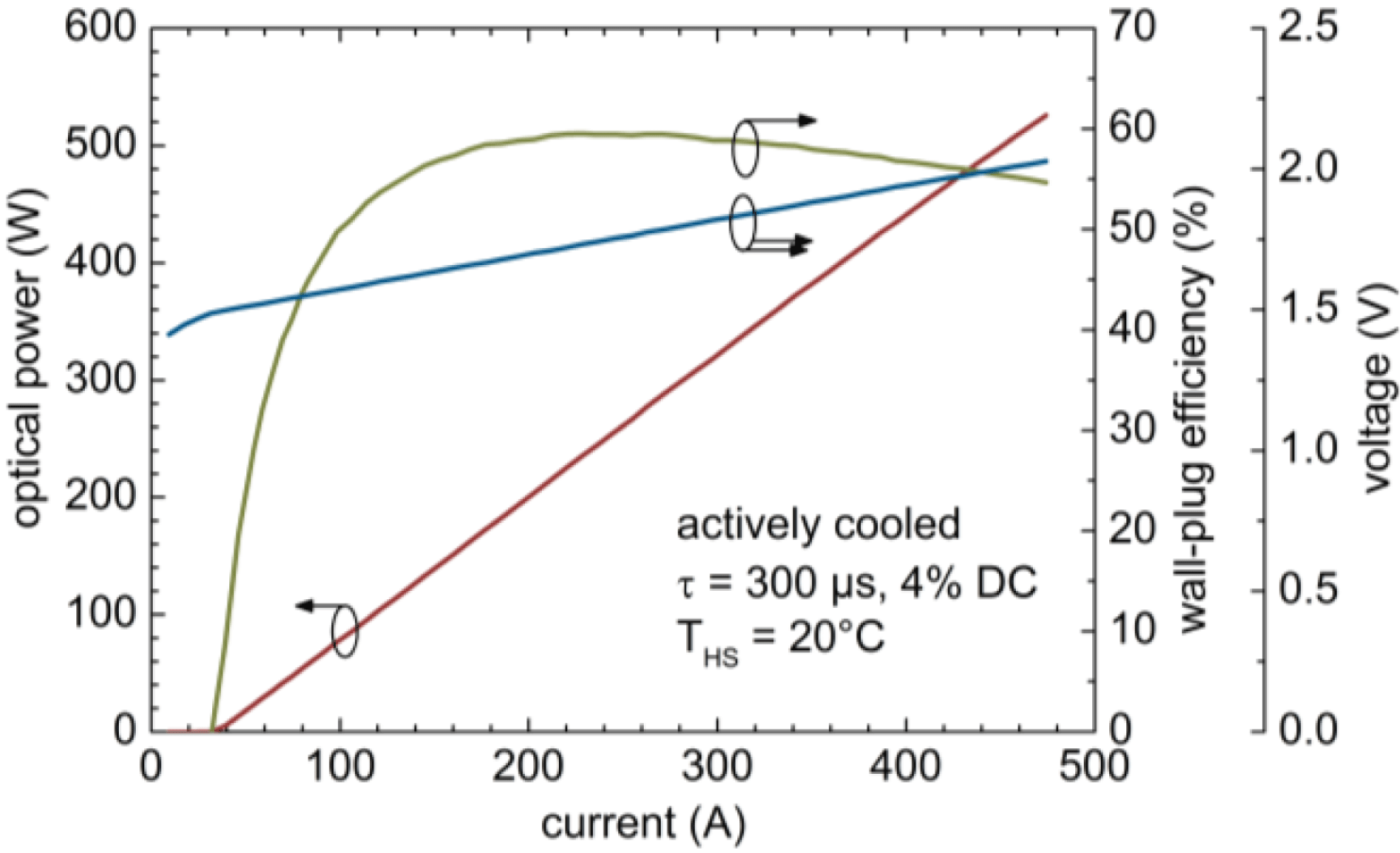
Figure 5. 880 nm QCW laser diode: light output power-versus-current characteristic and wall-plug efficiency.

Figure 6. Reliability testing of the 880 nm QCW laser diode in constant current mode, mounted on microchannel heatsinks. ![]() $T_{c}=25\,^{\circ }\text{C}$,
$T_{c}=25\,^{\circ }\text{C}$, ![]() ${\it\tau}=300~{\rm\mu}\text{s}$,
${\it\tau}=300~{\rm\mu}\text{s}$, ![]() $f=100~\text{Hz}$.
$f=100~\text{Hz}$.
3.3 940 nm QCW bars
The electro-optical performance of the new generation 940 nm QCW bars is shown in Figure 7. In agreement with the Yb pumping application, this device is characterized at ![]() ${\it\tau}=1~\text{ms}$[Reference Ertel, Banerjee, Mason, Phillips, Siebold, Hernandez-Gomez and Collier18]. The conversion efficiency at the operating point of 500 W is 53%. The latest improvements of this device are the narrow slow axis and fast axis divergence angles of the 37 emitter layout with 75% filling factor, as listed in Table 1. The spectrum of the 940 nm 500 W QCW bar has a width of 6.8 nm at 95% power content[Reference Pietrzak, Hülsewede, Zorn, Hirsekorn, Meusel, Kindsvater, Schröder, Blümel and Sebastian17], matching the requirement posed by the DiPOLE HEC-DPSSL installation.
${\it\tau}=1~\text{ms}$[Reference Ertel, Banerjee, Mason, Phillips, Siebold, Hernandez-Gomez and Collier18]. The conversion efficiency at the operating point of 500 W is 53%. The latest improvements of this device are the narrow slow axis and fast axis divergence angles of the 37 emitter layout with 75% filling factor, as listed in Table 1. The spectrum of the 940 nm 500 W QCW bar has a width of 6.8 nm at 95% power content[Reference Pietrzak, Hülsewede, Zorn, Hirsekorn, Meusel, Kindsvater, Schröder, Blümel and Sebastian17], matching the requirement posed by the DiPOLE HEC-DPSSL installation.

Figure 7. Power–voltage–current characteristics of 940 nm laser bars with 75% filling factor and 1.5 mm resonator length. ![]() ${\it\tau}=1~\text{ms}$,
${\it\tau}=1~\text{ms}$, ![]() $f=60~\text{Hz}$, 6% duty cycle,
$f=60~\text{Hz}$, 6% duty cycle, ![]() $T_{c}=25\,^{\circ }\text{C}$.
$T_{c}=25\,^{\circ }\text{C}$.
3.4 Outlook on the development of kW-class laser bars
For the case of 940 nm bars, we have recently analysed the possibility for scaling up to 1 kW pulse power, always keeping ![]() ${\it\tau}=1~\text{ms}$. To this end, we fabricated from different test structures long-cavity bars with 4 mm resonator length and 50% filling factor[Reference Pietrzak, Hülsewede, Zorn, Hirsekorn, Meusel, Kindsvater, Schröder, Blümel and Sebastian17]. In this test, the NG structure used in the 500 W bars was compared to structure C, as illustrated in Figure 8. The laser made with the NG structure has initially a higher slope up to 500 W, but then suffers from thermal rollover. Structure C is optimized against carrier leakage and achieves higher thermal stability. The conversion efficiency at high current density is increased compared to the NG structure, as shown in Figure 9, and reaches 58% at 900 W, 960 A.
${\it\tau}=1~\text{ms}$. To this end, we fabricated from different test structures long-cavity bars with 4 mm resonator length and 50% filling factor[Reference Pietrzak, Hülsewede, Zorn, Hirsekorn, Meusel, Kindsvater, Schröder, Blümel and Sebastian17]. In this test, the NG structure used in the 500 W bars was compared to structure C, as illustrated in Figure 8. The laser made with the NG structure has initially a higher slope up to 500 W, but then suffers from thermal rollover. Structure C is optimized against carrier leakage and achieves higher thermal stability. The conversion efficiency at high current density is increased compared to the NG structure, as shown in Figure 9, and reaches 58% at 900 W, 960 A.

Figure 8. Comparison of epitaxial structures for kW-class laser bars. The NG structure used in the 500 W bars is compared to structure C. ![]() ${\it\tau}=1~\text{ms}$,
${\it\tau}=1~\text{ms}$, ![]() $f=10~\text{Hz}$,
$f=10~\text{Hz}$, ![]() $T_{c}=25\,^{\circ }\text{C}$.
$T_{c}=25\,^{\circ }\text{C}$.

Figure 9. Wall-plug efficiency of 940 nm laser bars based on the NG epitaxial structure optimized structure C.
Our experiment shows that the output power per bar can be further increased if longer resonators are used. Higher output power densities can be achieved yet if the series resistance of the device can be drastically reduced, eliminating self-heating and thermal rollover. To this end, researchers from Ferdinand-Braun-Institut have recently proposed an epitaxial laser structure with a low-resistance waveguide[Reference Frevert, Bugge, Knigge, Ginolas, Erbert and Crump19]. Under the condition that the laser diodes are operated at ![]() $T_{c}=200~\text{K}$, the efficiency can thus be raised from 62% to 70% for 940 nm bars generating 1 kW light output at 1.2 ms pulse length. Cryogenic operation of the pump may be feasible in Yb:YAG amplifier systems, where the gain medium itself requires the cooling infrastructure. Use of this technology would benefit from a straightforward commercialization of the kW-class laser bars.
$T_{c}=200~\text{K}$, the efficiency can thus be raised from 62% to 70% for 940 nm bars generating 1 kW light output at 1.2 ms pulse length. Cryogenic operation of the pump may be feasible in Yb:YAG amplifier systems, where the gain medium itself requires the cooling infrastructure. Use of this technology would benefit from a straightforward commercialization of the kW-class laser bars.
4 Laser diode stacks
Integration of laser diode chips in high-power applications requires dense array packaging. Laser diode stacks provide electrical contact, cooling and, optionally, fast axis collimation. The maximum packaging density of laser diode chips depends on the efficiency of the cooling system. An example of dense stacking and cooling with a water passage is the JenLas® QCW Cool laser diode stack, shown in Figure 10. Laser diode stacks for short-pulse operation, QCW stacks, are available in a ‘passive’ version with conductive cooling by mounting on a cool surface, and in an ‘active’ version with an integrated water passage. Figure 11 shows a cross-section of an active QCW stack and mount illustrating the water passage.
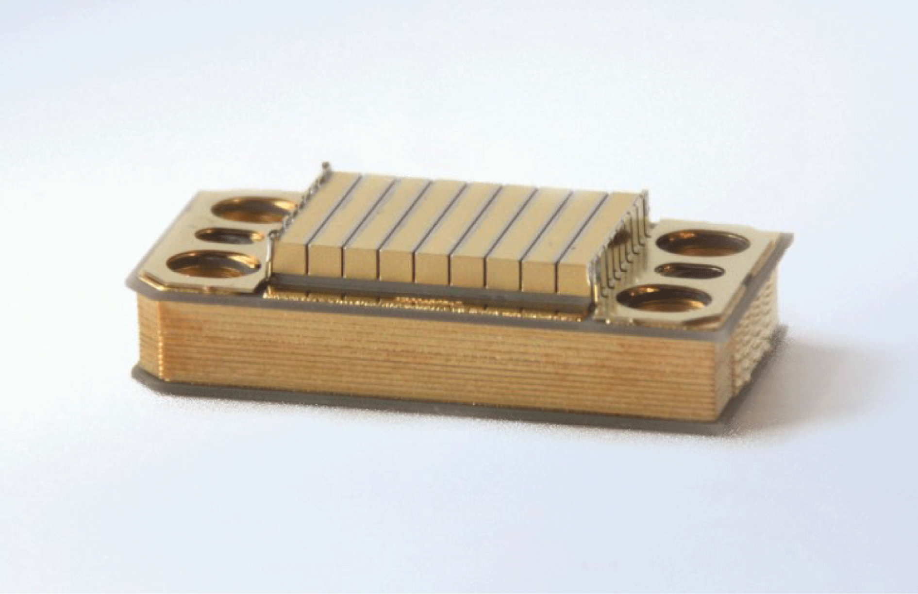
Figure 10. Photograph of JenLas® QCW Cool laser diode stack with 8 laser bars spaced at 1.7 mm pitch.
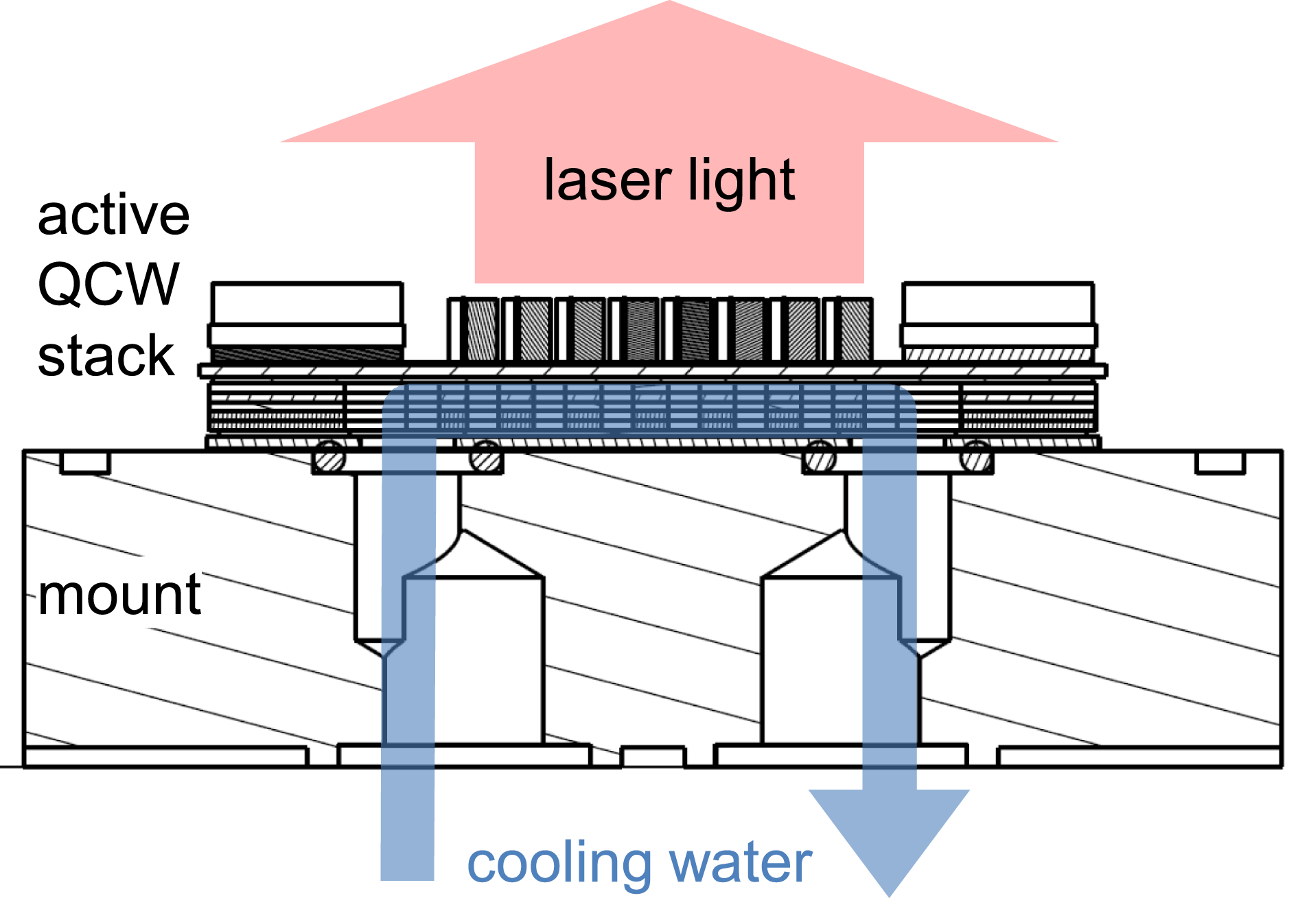
Figure 11. Cross-section of actively cooled QCW stack on mount with illustration of the water passage.

Figure 12. Transient thermal behaviour of the passively cooled QCW stack, showing the thermal impedance ![]() $Z_{\mathit{th}}(t)$ of one laser bar. The CW operating temperature is attained after 3 s.
$Z_{\mathit{th}}(t)$ of one laser bar. The CW operating temperature is attained after 3 s.
Semiconductors have a limited operating temperature, and therefore the maximum light output power of a laser in continuous operation depends on the net transport of waste heat by the cooler. In contrast, QCW operation permits to store the waste heat in the package and remove the heat between pulses. The local heat capacity is therefore a factor of similar importance to the thermal resistance from diode chip to coolant. The resulting transient thermal behaviour of the diode module is best represented by the thermal impedance function ![]() $Z_{\mathit{th}}(t)$, giving the temperature rise for 1 W heat dissipation immediately after turn-on.
$Z_{\mathit{th}}(t)$, giving the temperature rise for 1 W heat dissipation immediately after turn-on. ![]() $Z_{\mathit{th}}(t)$ is shown in Figure 12 for three different QCW stacks. The data was obtained by finite element modelling. The thermal behaviour of the passive stack with 1.7 mm bar-to-bar pitch is indicated by the dashed line. At
$Z_{\mathit{th}}(t)$ is shown in Figure 12 for three different QCW stacks. The data was obtained by finite element modelling. The thermal behaviour of the passive stack with 1.7 mm bar-to-bar pitch is indicated by the dashed line. At ![]() $t=3$ s, thermal equilibrium is reached, the thermal capacitances adjacent to the laser bar are fully heated, and the temperature rise per Watt of dissipated heat corresponds to the thermal resistance
$t=3$ s, thermal equilibrium is reached, the thermal capacitances adjacent to the laser bar are fully heated, and the temperature rise per Watt of dissipated heat corresponds to the thermal resistance ![]() $R_{\mathit{th}}=5.3~\text{K}/\text{W}$ per laser bar. The temperature difference is measured between the semiconductor laser bar and the cooler surface, and contains the temperature drop across a thermal conductive foil (
$R_{\mathit{th}}=5.3~\text{K}/\text{W}$ per laser bar. The temperature difference is measured between the semiconductor laser bar and the cooler surface, and contains the temperature drop across a thermal conductive foil (![]() $0.01~\text{W}/\text{mm}^{2}/\text{K}$)[Reference Wölz, Zorn, Pietrzak, Kindsvater, Meusel, Hülsewede and Sebastian20]. The
$0.01~\text{W}/\text{mm}^{2}/\text{K}$)[Reference Wölz, Zorn, Pietrzak, Kindsvater, Meusel, Hülsewede and Sebastian20]. The ![]() $Z_{\mathit{th}}(t)$ data for two active stacks is also shown. The direct water passage into the stack permits much lower equilibrium temperature gradients between the semiconductor and the cooling water, with
$Z_{\mathit{th}}(t)$ data for two active stacks is also shown. The direct water passage into the stack permits much lower equilibrium temperature gradients between the semiconductor and the cooling water, with ![]() $R_{\mathit{th}}=1.3~\text{K}/\text{W}$ per bar for 1.7 mm pitch and
$R_{\mathit{th}}=1.3~\text{K}/\text{W}$ per bar for 1.7 mm pitch and ![]() $R_{\mathit{th}}=1.8~\text{K}/\text{W}$ per bar for 1.2 mm pitch. It can be noted in Figure 12 that the reduced pitch of 1.2 mm leads to faster heating from about 10 ms onwards, due to the reduced heat capacity between the substrates. On the other hand, it is also apparent that the effect can be neglected for high-power laser pumping applications operating at low duty cycles, because the pulse widths are much below 10 ms.
$R_{\mathit{th}}=1.8~\text{K}/\text{W}$ per bar for 1.2 mm pitch. It can be noted in Figure 12 that the reduced pitch of 1.2 mm leads to faster heating from about 10 ms onwards, due to the reduced heat capacity between the substrates. On the other hand, it is also apparent that the effect can be neglected for high-power laser pumping applications operating at low duty cycles, because the pulse widths are much below 10 ms.
The temperature profile for arbitrary pulse patterns can be calculated from ![]() $Z_{\mathit{th}}(t)$[Reference Schweitzer21]. An illustration is given by Figure 13, showing the temperature rise per 1 W heat dissipation for a passive QCW stack with 1.7 mm pitch, operated with
$Z_{\mathit{th}}(t)$[Reference Schweitzer21]. An illustration is given by Figure 13, showing the temperature rise per 1 W heat dissipation for a passive QCW stack with 1.7 mm pitch, operated with ![]() ${\it\tau}=300~{\rm\mu}\text{s}$ at different duty cycles. Considering that high-power laser applications dissipate several hundred Watt of heat during each pulse, and that the lifetime of GaAs-based semiconductor lasers decreases exponentially with temperature, it is clear that active cooling is essential for high duty cycle operation.
${\it\tau}=300~{\rm\mu}\text{s}$ at different duty cycles. Considering that high-power laser applications dissipate several hundred Watt of heat during each pulse, and that the lifetime of GaAs-based semiconductor lasers decreases exponentially with temperature, it is clear that active cooling is essential for high duty cycle operation.
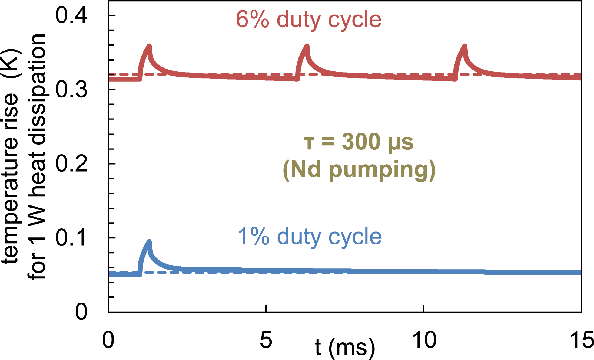
Figure 13. Temperature gradient in pulsed operation of the QCW stack with power dissipation of 1 W per bar during ![]() ${\it\tau}=300~{\rm\mu}\text{s}$. The solid lines denote the exact temporal evolution. The dashed lines show the product of
${\it\tau}=300~{\rm\mu}\text{s}$. The solid lines denote the exact temporal evolution. The dashed lines show the product of ![]() $R_{\mathit{th}}$ and the duty cycle.
$R_{\mathit{th}}$ and the duty cycle.
We give some examples of the array irradiance achieved by currently available diode modules in Figure 14. Direct stacking of the laser bars (NGCEO) results in power densities of ![]() $20~\text{kW}/\text{cm}^{2}$, but is feasible only for very short-pulse lengths, because of the absence of significant heat capacity between bars. For cases where more heat must be stored, the chips are mounted on spacers at pitches of 0.33 mm (Quantel), 0.4 or 1.7 mm, for example. An increase in maximum pulse power is then possible by increasing the power per chip, indicated by the dashed lines. Jenoptik’s NG 500 W QCW laser diode bars push the array power density for 0.4 mm pitch to
$20~\text{kW}/\text{cm}^{2}$, but is feasible only for very short-pulse lengths, because of the absence of significant heat capacity between bars. For cases where more heat must be stored, the chips are mounted on spacers at pitches of 0.33 mm (Quantel), 0.4 or 1.7 mm, for example. An increase in maximum pulse power is then possible by increasing the power per chip, indicated by the dashed lines. Jenoptik’s NG 500 W QCW laser diode bars push the array power density for 0.4 mm pitch to ![]() $12.5~\text{kW}/\text{cm}^{2}$.
$12.5~\text{kW}/\text{cm}^{2}$.

Figure 14. Pump power densities achieved with commercially available laser diodes. Squares: JENOPTIK, circles: NGCEO ARR179P6000HDS and Quantel QD-Q5912-B.
The NG 500 W bars can be combined in QCW stacks, as illustrated in Figure 15 by the measurements on a passive 8-bar stack emitting at 880 nm. The linear power–current characteristic known from the laser bar characterization above scales up to 4 kW light output from the stack at a duty cycle of 1% with pulses of ![]() ${\it\tau}=300~{\rm\mu}\text{s}$ at 33 Hz. In agreement with the calculation of the temperature profile in Figure 13, increasing the duty cycle further leads to thermal rollover in this passive stack. The duty cycle required in the nuclear fusion application mentioned above, however, is lower.
${\it\tau}=300~{\rm\mu}\text{s}$ at 33 Hz. In agreement with the calculation of the temperature profile in Figure 13, increasing the duty cycle further leads to thermal rollover in this passive stack. The duty cycle required in the nuclear fusion application mentioned above, however, is lower.

Figure 15. Electro-optical data of a passively cooled QCW stack with eight laser bars emitting at 880 nm, ![]() ${\it\tau}=300~{\rm\mu}\text{s}$, bar-to-bar pitch 1.7 mm, duty cycle (d.c.) varied between 1% and 10%. (The step in efficiency at 450 A is a measurement artefact.)
${\it\tau}=300~{\rm\mu}\text{s}$, bar-to-bar pitch 1.7 mm, duty cycle (d.c.) varied between 1% and 10%. (The step in efficiency at 450 A is a measurement artefact.)
The development in high-power laser diodes, as well as the progress in the existing HEC-DPSSL installations described above, put the IFE lasers technologically within reach. In the following sections, we describe our vision of the increase in semiconductor laser supply that is an obvious prerequisite for an IFE power plant.
5 Manufacturing environment for high-power laser diodes
As we had shown in Table 1, the requirement in the LIFE scenario exceeds today’s total worldwide annual production capacity for high-power laser bars by far. In a gedankenexperiment, we suggest a development of the laser diode market similar to high-brightness light-emitting diodes (LEDs). This seems a reasonable approximation, because the crystal growth tools (metal–organic chemical vapour deposition, or MOCVD) are the biggest capital investment in the factory, and are identical for making laser bars or red LEDs on GaAs wafers. In Figure 16, we compare today’s worldwide high-power laser diode production capacity to the one-time requirements for one LIFE or HiPER plant and to the estimated development of the red (InGaAlP) LED production[22], in the equivalent of ![]() $4^{\prime \prime }$ wafers. The estimates are based on 20 MOCVD tools used today by all manufacturers for laser bar production on
$4^{\prime \prime }$ wafers. The estimates are based on 20 MOCVD tools used today by all manufacturers for laser bar production on ![]() $3^{\prime \prime }$ wafers, compared to 400 tools for red LEDs on
$3^{\prime \prime }$ wafers, compared to 400 tools for red LEDs on ![]() $4^{\prime \prime }$ wafers. It is apparent from Figure 16 that the diode chips for HiPER could be produced with today’s equipment. For LIFE, on the other hand, diode production would take ten years, assuming that nothing else is made. Interestingly, the challenge is much less if seen from an LED manufacturer’s perspective: on today’s machinery, and given the current rapid development of the LED production volume, the laser diode chips for LIFE could be made ‘immediately’. A decay of the dollar-per-lumen value by a factor of ten per decade has been observed in the history of red LEDs[Reference Haitz and Tsao23]. We tentatively conclude that a demand for laser bars on the LIFE plant scale would have similar drastic effects on production cost, given only the scaling effects of the industry. This price reduction, however, may still fall short of the goal stated in Table 1, and we propose in Section 6 how to go a step further.
$4^{\prime \prime }$ wafers. It is apparent from Figure 16 that the diode chips for HiPER could be produced with today’s equipment. For LIFE, on the other hand, diode production would take ten years, assuming that nothing else is made. Interestingly, the challenge is much less if seen from an LED manufacturer’s perspective: on today’s machinery, and given the current rapid development of the LED production volume, the laser diode chips for LIFE could be made ‘immediately’. A decay of the dollar-per-lumen value by a factor of ten per decade has been observed in the history of red LEDs[Reference Haitz and Tsao23]. We tentatively conclude that a demand for laser bars on the LIFE plant scale would have similar drastic effects on production cost, given only the scaling effects of the industry. This price reduction, however, may still fall short of the goal stated in Table 1, and we propose in Section 6 how to go a step further.
6 Standardization
Competition between industrial suppliers promotes non-compatible in-house standards but also reduces the size of production batches and finally limits the potential for cost reduction. As a way out, we propose to initiate a standardization discussion. This process could help to enlarge capacities by bundling the capability of multiple suppliers on a short track, and could also reduce commercial and technical risks by larger batch sizes for high-power laser diodes. Within the frame of this work pulsed laser diode stacks are considered as a pumping source for a solid-state laser. This leads to a number of functionalities which have to be met, and are illustrated in Figure 17.

Figure 17. Functionalities of a diode laser pump.

Figure 18. Utilization aspects of standardization at different levels.
In a lot of cases these functionalities will be fulfilled by technical solutions, which are produced by specialized suppliers. It is obvious, that standardization of one component may guide to standardization of the components in its functional environment. As an example the standardization at the laser diode level may also trigger standardization for stack geometry and its mechanical fixing, the electrical and cooling supply specifications, optical beam shaping, etc., but also operational modes and maintenance services.
In Figure 18 some effects of standardization to the partners in the utilization chain are analysed. As an example, standardization means for component suppliers larger batch sizes, reduced variants, better reproducibility and higher yield. A system integrator benefits, among other aspects, from compatibility between multiple suppliers. For the user, these levers finally act on cost.
It is clear, that standardization would require an active search for common specifications at the side of public users, i.e., the research projects, as well as a discussion of the adequate technological solution under commercial aspects at the producers’ side. This process could be moderated by international authorities like IAEA or EURATOM and implemented into funded project calls.
7 Conclusion
Laser diodes have been identified as one of the critical factors for inertial confinement fusion. Given the progress with scalable HEC-DPSSL installations worldwide and the current laser diode technology, the projected technical requirements from the LIFE and HiPER studies can be met. By analogy to the LED market, we suggest that the industry will also be able to sufficiently ramp up production. In addition, we envisage a standardization programme to lower IFE plant construction and operation cost.

