1. Introduction
Various groups Reference Nakamura, Senoh, Iwasa, Nagahama, Yamada and Mukai[1] Reference Ponce and Bour[2] Reference Osinski and Barton[3] Reference Egawa, Ishikawa, Jimbo and Umeno[4] Reference Osinski, Zeller, Chiu, Phillips and Barton[5] have studied the problem of GaN-based light-emitting diode (LED) degradation in the last few years, but mechanisms of degradation are not yet understood. The goal of the present work was a research of aging processes in LED’s for which luminescence and electrical properties were investigated in Reference Zolina, Kudryashov, Turkin, Yunovich and Nakamura[6] Reference Zolina, Kudryashov, Turkin and Yunovich[7] Reference Yunovich, Kovalev, Kudryashov, Manyachin, Turkin and Zolina[8] Reference Kudryashov, Zolina, Turkin, Yunovich, Kovalev and Manyakhin[9] Reference Manyakhin, Kovalev, Kudryashov, Turkin and Yunovich[10]. Preliminary results of this study were published in references Reference Kovalev, Kudryashov, Manyakhin, Turkin and Yunovich[11] Reference Kovalev, Kudryashov, Manyakhin, Turkin and Yunovich[12]. The experiments were done at moderately high currents, not far from the normal LED operating conditions. Changes of LED properties were observed over 102−103 hours. Models are proposed to explain these changes.
2. Experimental
Blue and green LED’s based on InxGa1−xN/AlyGa1−y/GaN heterostructures were studied; Dr. S. Nakamura (Nichia Chemical Co) has sent the samples to us. Reference Nakamura, Senoh, Iwasa, Nagahama, Yamada and Mukai[1] Reference Zolina, Kudryashov, Turkin, Yunovich and Nakamura[6] The heterostructures had an InGaN single quantum well active layer with thickness d ≈ 3.5 nm; the properties of these diodes were studied in references Reference Zolina, Kudryashov, Turkin, Yunovich and Nakamura[6] Reference Zolina, Kudryashov, Turkin and Yunovich[7] Reference Yunovich, Kovalev, Kudryashov, Manyachin, Turkin and Zolina[8] Reference Kudryashov, Zolina, Turkin, Yunovich, Kovalev and Manyakhin[9] Reference Manyakhin, Kovalev, Kudryashov, Turkin and Yunovich[10].
The choice of aging conditions was made as follows. Estimations of changes of the LED characteristics were carried out while increasing the constant current over the range J=10−100 mA. Remarkable changes of spectra, capacitance-voltage (C(V)) and current-voltage (J(V)) characteristics were detected at 60−100 mA for hundreds of hours. A constant current J=80 mA was chosen for further experiments. The temperature of the LED’s active area was estimated from the spectra at 80 mA to be T = 360−370 K Reference Kovalev, Kudryashov, Manyakhin, Turkin and Yunovich[12]. The tests were carried out over 2000 hours. An essential part of the work was a study of the distributions of charged center effective concentration (CCEC) in the space charge region during aging.
The measurement technique is described in reference Reference Manyakhin, Kovalev, Kudryashov, Turkin and Yunovich[13]. If the DC voltage on a p-n-junction is V and an AC voltage of small amplitude ΔV induces a small change of a charge ΔQ, then we can use an equation:
(W- width of the space charge region, S - a square of the structure, ε - dielectric constant, e -electron charge, N - concentration of the charged centers). Two voltages, ΔVW and ΔVN, were measured separately using an AC charge·ΔQ of constant amplitude as a sum of two high frequency signals of nearby frequencies ω1 and ω2. The signal ΔVN was measured at the frequency Ω = (ω1 − ω2); the signal ΔVW was measured at the frequency (ω1 + ω2)/2. Values of W and N, calculated from ΔVW and ΔVN at different V, were plotted as curves N(W).
3. Experimental results
3.1 Changes of electroluminescence spectra
The intensity of EL spectra at 15 mA increased by 10 + 40 % within the first 50−100 hours of operation (at 80 mA) for blue LED’s and within ≈ 800 hours for green LED’s. The intensity fell slowly during the following period, ≈ 800−1000 hours for blue and > 1000 hours for green LED’s (see Reference Manyakhin, Kovalev, Kudryashov, Turkin and Yunovich[10] Reference Kovalev, Kudryashov, Manyakhin, Turkin and Yunovich[11]). The strong changes of the spectra were detected for blue LED’s at low currents, J < 0.15 mA, where the tunnel and the injection components of the current are of the same order of magnitude. The intensity of luminescence decreased, but the relative intensity of the tunnel band (studied in Reference Zolina, Kudryashov, Turkin, Yunovich and Nakamura[6] Reference Zolina, Kudryashov, Turkin and Yunovich[7] Reference Yunovich, Kovalev, Kudryashov, Manyachin, Turkin and Zolina[8] Reference Kudryashov, Zolina, Turkin, Yunovich, Kovalev and Manyakhin[9] Reference Manyakhin, Kovalev, Kudryashov, Turkin and Yunovich[10]) increased about three times (see Figure 1).
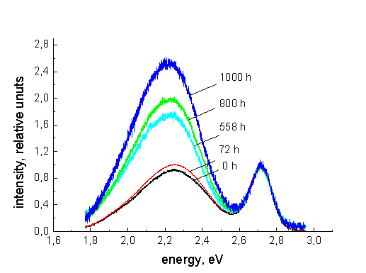
Figure 1a. Luminescence spectra of a blue LED at J = 0.15 mA( spectra are normalized at the maximum of the blue line); numbers at the curves are the hours of aging at J = 80 mA.
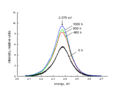
Figure 1b. Luminescence spectra of a green LED at J = 0.15 mA; numbers at the curves are hours of aging at J = 80 mA.
The intensity of the breakdown luminescence spectra (studied in Reference Manyakhin, Kovalev, Kudryashov, Turkin and Yunovich[10]) decreased in the process of aging. But the relative intensity of a yellow band (2.1−2.3 eV) increased (see Figure 2). It is known that the yellow band is caused by complexes with structural defects Reference Kudryashov, Zolina, Turkin, Yunovich, Kovalev and Manyakhin[9]; we conclude that defects are created on the borders of the space charge region, where the recombination take place.
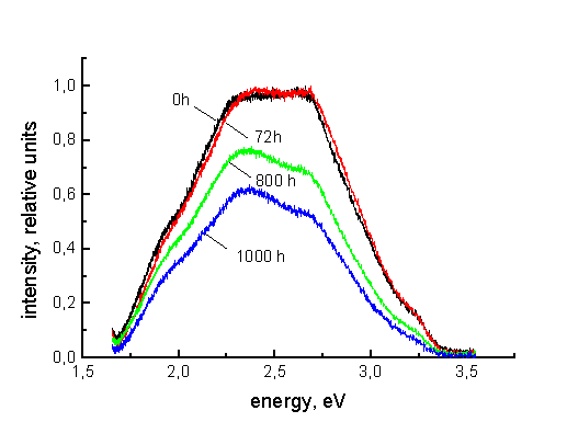
Figure 2. Breakdown luminescence spectra of a blue LED at J = − 4 mA; numbers at the curves are hours of aging at J = 80 mA.
3.2 Changes of electrical properties
The changes of J(V) during aging are shown in Figure 3. A tunnel component of the direct current at low V grew both for blue and green LED’s. The series resistance Rs (sufficient at higher J) grew during the 2nd period of aging. Defect formation depended on Rs (see the discussion below).
The effective concentration of charged acceptors on the p-side of the blue LED’s junction grew by 10−15% during the 1st period of aging; during the 2nd period (≈ 1000 hours) it fell (see Figure 4). The width of the space charge region grew by only ≈ 30%. The CCEC of green LED’s slowly grew for 600−800 hours by ≈ 10 % and after that fell insignificantly. It is to be noted that the change of CCEC takes place over a distance W ≈ 40−80 nm, of the same order of magnitude as a mean free path 1fp (see an estimation below).
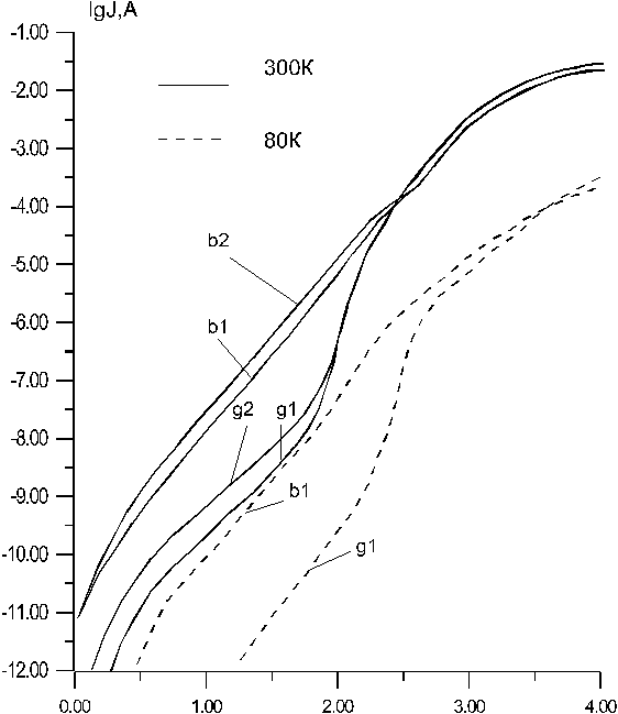
Figure 3. Current-voltage characteristics of a blue (b) and a green (g) LED’s before (1) and after (2) aging at J = 80 mA during 800 hours.
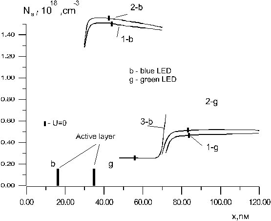
Figure 4. Distribution of the effective charged centers concentration on the p-side of the space charge region of blue (b) and green (g) LED’s before and after aging at J = 80 mA: 1) t=0; 2) t=250 hours; 3) t=1000 hours.
4. Discussion
4.1 Model of growth and fall of the luminescence efficiency
A model of the 1st stage may be as follows. There are residual complexes Mg-H in the active layer; electrons at high injection currents can disrupt them so, that the hydrogen goes out of complexes and the charge of Mg-ions should be compensated by holes:
We suppose that in the 2nd stage the formation of donor defects which compensate acceptors prevails. A possible defect may be the Nitrogen vacancy - VN; the probability of VN formation in p-type GaN is appreciably higher than that of Gallium vacancies Reference Manyakhin, Kovalev, Kudryashov, Turkin and Yunovich[10] Reference Kovalev, Kudryashov, Manyakhin, Turkin and Yunovich[11]:
These defects increase the probability of nonradiative recombination. The sign of the charges in this equation are given conditionally, they are not confirmed. Such a model explains the second stage of the aging process. In addition, there takes place a migration of defects on the borders of growth columns: the defects accumulate in “weak points” of maximal electrical field. It is possible in such a way to explain the growth of the tunnel components of the current and spectra.
4.2 Formation of sub-threshold defects by electron injection
The formation of structural defects in GaN at a rather low temperature (about T=370 K) needs to be explained. This is possible by using a model of defect creation by hot electrons in p-n heterostructures. This model was developed for GaAs-based structures and has explained the aging processes in n-AlGaAs/p-GaAs heterojunctions rather well Reference Manyachin[14]. It is supposed that the electrons receive an additional kinetic energy crossing the heterojunction with a conduction band offset. These hot electrons transfer the energy to the atoms that are displaced. The assumption is based on the experimental fact that the defects are formed over a depth of about the mean free path lfp from the heterojunction boundary (not on the diffusion length, Ln >> 1fp).
Electrons injected from the n-side of a heterojunction into the p-layer have an energy ΔE relative the bottom of the conduction band in the quantum well: ΔE >> kT:
Electrons should give this energy back at the other side of a well (on the p-side, see Figure 5a). The average energy of electrons remains the same as on the n-boundary at a voltage of about a contact potential, V ≈ φk(see Figure 5b). There are compensated layers in the investigated structures on both sides of the quantum well Reference Zolina, Kudryashov, Turkin and Yunovich[7] Reference Yunovich, Kovalev, Kudryashov, Manyachin, Turkin and Zolina[8] Reference Kudryashov, Zolina, Turkin, Yunovich, Kovalev and Manyakhin[9] Reference Manyakhin, Kovalev, Kudryashov, Turkin and Yunovich[10]. At V > φk most of the forward voltage falls on the quantum wells in the layers. Electrons get additional energy in the electrical field of the compensated layers over a mean free path lfp (see Figure 5c).
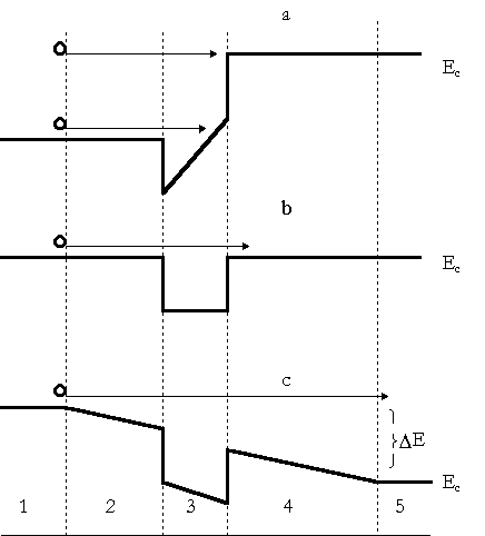
Figure 5. A model of electron transfer from the n- to the p-side of the heterojunction with a compensated layer: a) - at U<ϕk, b) at U≈ ϕk, c) at U>ϕk; 1 - n-GaN; 2,4 - compensated layers; 3 - InGaN (the active layer), 5 - p-AlGaN.
Kinetic energy of electrons at a high current density can be transferred to a lattice during the relaxation time on a length of the order lfp not only by phonon scattering, but also by sub-threshold defect formation. It should occur either in the compensated layers near the active layer, or in the p- space charge layer.
If electrons transfer energy to the Mg-H complexes, the reaction of breaking the complex and activating the Mg-acceptor (equation 1) will go with a high probability. This mechanism will take place mainly on the border of the active layer in p-AlGaN. The threshold energy Ed of breaking the complex Mg-H is greater than the thermodynamic Frenkel energy; estimates have given a value of Ed ≈ 4 eV.
It is known that at high temperatures nitrogen leaves the GaN lattice as a gas, N2, forming vacancies VN Reference Vartuli, Pearton, Lambers, Abernathy, MacKenzie and Zolper[15]. If hot electrons transfer an energy to the lattice breaking the Ga-N bond, the formation reaction for defects (equation 2) will occur at lower T. It is to be noted that the formation probability of equilibrium donor vacancies VN is higher in p-GaN Reference Van De Walle, Stampfl and Neugebauer[16].
The processes of Mg- activation and VN creation are simultaneous. At the 1st stage the Mg- activation prevails, but it is limited by a low Mg-H concentration. At the 2nd stage the VN creation prevails and it is not limited: N- atoms are intrinsic in the lattice. A dynamic equilibrium concentration of N- vacancies will be established at a long aging time.
4.3 Analysis of the sub-threshold defect formation
4.3.1. Probability of atom displacement by hot electrons
The theoretical analysis will be done for sub-threshold defect formation during hot electron injection by an analogy with the theories of the high energy particle interactions with atoms of a crystal Reference Vavilov, Kiv and Niyazova[17]. The main difference consists of the fact that the energy of hot electrons, ΔE, is orders of magnitude less than the threshold energy Ed of atom displacement. In this case the process of interaction goes through the excitation of an electronic subsystem Reference Vavilov, Kiv and Niyazova[17] Reference Vavilov[18]. The displacement of atom in a lattice by electrons with kinetic energy ΔE has a probability:
where Ed is the displacement threshold energy. The effective probability of displacement integrated over all energies ΔE and velocities vx, is equal to
where νi = mn*vi 2/2kT, f0 is the distribution function of electrons in the n-emitter, and vi are components of the electron’s thermal velocity.
4.3.2. Distribution of created defects versus time and distance
Let’s assume that the diffusion of generated defects is low, and we may neglect the electrical field in the considered area. Then the concentration of the displaced intrinsic atoms ΔN0 changes in time t and distance x according to the equations:

where N0 is the concentration at the time t=0, a(x) is the spatial distribution of the generation rate of point defects, G(x) is their generation rate, j = J/S is the current density, q is the electron charge. τ0 is the characteristic relaxation time of defect displacement, LD is the diffusion length, σ0 is the cross-section of hot electron interaction with the atom. This dependence will saturate with time with a time constant τ0(T).
The change of concentration of Mg-H complexes, whose concentration is less than the concentration of intrinsic atoms, Nc << N0, is described by an equation:
where γk(x) and τk(T) are analogous to the parameters γ0(x) and τ0(T) in equation 6. The dependence ΔNk (x, t) is described by the equation
It is assumed in this equation that the concentration Nk0 is rather low and that the hydrogen atoms have a high probability to exit the lattice at high values of τk(T).
The value of the mean free path lfp is of the order lfp≈ 3.10−6 cm; it is included in the expression for a(x) assuming an electron mobility of 400−600 cm2/V·s which is determined mainly by the lattice phonon scattering. The interaction cross-section σ0= (Nolfp )−1may be assumed to be ≈ 9−10−17 cm2. Let us take values of t≈τ0≈102−103 hours from our experiments at J = 80 mA (j = 80 A/cm2) for blue LED’s.
It is then possible to estimate the threshold energy and effective probability of displacement of atoms, ξ0 in equation 6: Ed ≈ 7−8 eV; ξ0≈ 2·10−14. Estimates of the effective probability of atoms displacement for Mg-H complexes give these parameter values: Ed ≈3−4 eV; γk≈10−5, ξk≈8·10−10. These values are used for an explanation of the changes of the concentration of the charged impurity ΔN0, ΔNk in the described experiments.
A dependence ΔN(t) was calculated using equation 7 and equation 8 with the parameters estimated above (see Figure 6). The points on the curves correspond to the measurements given in Figure 4 for blue and green LED’s; the changes of effective charge concentration are close to the calculated curves.

Figure 6. Changes of the effective concentration of charged centers in the space charge region of heterojunctions of blue (upper, at x = 0.67 lfp, a) ) and green (lower, at x = 3 lfp, b) LED’s, lfp≈ 3.10−6 cm. Values of x and points -squares- experimental data (Figure 4); points - circles luminescent intensity at J = 15 mA (right scale); curves - calculations by equations (6−8).
Our estimates give only orders of magnitude of the parameters. They only show that sub-threshold creation of point defects by injected hot electrons in GaN heterostructures can explain LED aging effects.
5. Conclusions
Luminescence spectra and electrical properties of blue and green LED’s based on InGaN/AlGaN/GaN heterostructures with single quantum wells change remarkably within 100 −2000 hours of operatingat a current 80 mA.
An increase of luminescence intensity at currents ≈15 mA and an increase of charged acceptor concentration in the space charge region during the first period of aging is explained by activation of Mg acceptors due to an exit of H atoms from residual Mg-H complexes.
The slow fall of luminescence intensity and charged acceptor concentration during the second period can be explained by creation of donor defects by injection of hot electrons into quantum wells. The first period for blue diodes is shorter (70−100 hours.) than it is for green ones (800−1000 hours), which is caused by the greater compensation of acceptors and lower electric fields in the green diodes.
A model of injection stimulated sub-threshold formation of defects (breaking of bonds Mg-H or bonds Ga-N by hot electrons injected into quantum wells) can explain effects of aging.
Acknowledgments
Authors are grateful to Dr. S. Nakamura (Nichia Chemical Co. Ltd.) for sending LED’s to Moscow University; to Professor V. S. Vavilov for discussions; to V. E. Kudryashov and A. N. Turkin for a help in experiments. A. E. Yunovich thanks the International Soros Science Education Program for financial support.


