


1 Introduction
Optical films are commonly used for core components of high-precision, high-power laser instruments, such as gravitational wave interferometers, laser gyroscopes, laser inertial confinement fusion, laser communication devices and laser ranging systems[ Reference Zhang, Xian, Wang and Zhan 1 – Reference Murphy, Adelberger, Battat, Hoyle, Johnson, Mcmillan, Michelsen, Stubbs and Swanson 6 ]. When a high-energy laser acts on optical film, the film absorbs laser energy and causes the temperature to rise, resulting in deformation and a decrease in the performance of the optical system[ Reference Li, Niu, Xia, Jiao, Dun, Zhang, Cheng and Wang 7 ]. Therefore, to control the temperature rise of optical components during the operation of high-power laser systems and consequently improve beam quality and power density, it is essential to enhance the ability of thin film materials to suppress optical absorption.
Tantalum pentoxide (Ta2O5) has high transparency from the near-ultraviolet to infrared bands, making it a commonly used high-refractive-index material in laser thin films[ Reference Wen, Zhu, Sun, Li and Shao 8 ]. Ta2O5 exhibits common challenges associated with metal oxides, particularly the difficulty in avoiding oxygen vacancies, which makes it difficult to reduce the absorption of the film[ Reference Guo and Robertson 9 ]. Currently, doping and annealing are effective methods for suppressing thin film absorption. Annealing, by promoting extended relaxation, aids in stress release and the reduction of defects within the thin film structure[ Reference Ren, Yang, Feng, Miao, Xia and Wang 10 , Reference Lv, Huang, Zhang, Deng, Gong, Wang, Pan, Li and Jin 11 ]. Chen et al. [ Reference Chen, Wang, Feng, Wang, Chen, Lu, Zhang, Li, Cui and Shao 12 ] prepared Ta2O5 film using a double-ion beam sputtering (IBS) deposition system. The absorption of the film decreased after heat treatment. Under the process conditions of 35 sccm (standard cubic centimeters per minute) of ionized oxygen and 40 sccm of oxygen flow, the film exhibited a low absorption of 1.2 ppm (parts per million) after annealing at 400°C. However, it is generally challenging to completely eliminate defects in the film using annealing alone[ Reference Sayah, Sassolas, Degallaix, Pinard, Michel, Sordini and Cagnoli 13 ]. Doping is widely recognized as an effective method for reducing thin film absorption. Elements such as Ti, Zr, W, Co, Hf and Si can be introduced as dopants during the deposition process, modifying the film’s structure and absorption properties[ Reference Salam, Fukuda and Nomura 14 – Reference Wen, Zhu, Chai, Liu, Shi, Du and Shao 16 ]. Wen et al. [ Reference Harry, Abernathy, Becerra-Toledo, Armandula, Black, Dooley, Eichenfield, Nwabugwu, Villar, Crooks, Cagnoli, Hough, How, MacLaren, Murray, Reid, Rowan, Sneddon, Fejer, Route, Penn, Ganau, Mackowski, Michel, Pirand and Remillieux 17 ] and Harry et al. [ Reference Jacoby 18 ] prepared Ta2O5 films with different concentrations of doped TiO2 by IBS and found that doping reduced the internal loss of the coating and the minimum absorption of the film could reach 0.9 ± 0.1 ppm, which is close to meeting the light absorption requirements of second-generation gravitational wave detectors. Doping will affect the optical absorption properties of the film, but there is currently no clear explanation for its influence rules and mechanisms.
The primary deposition techniques used for optical thin films include IBS, reactive magnetron sputtering, electron-beam evaporation and atomic layer deposition[ Reference Molina-Ruiz, Shukla, Ananyeva, Vajente, Abernathy, Metcalf, Liu, Markosyan, Bassiri, Fejer, Fazio, Yang, Menoni and Hellman 19 – Reference Kochanneck, Rönn, Tewes, Hoffmann, Virtanen, Maydannik, Sneck, Wienke and Ristau 23 ]. IBS is currently the primary method for fabricating ultra-low-absorption films. This technique produces samples with smooth surfaces and dense structures[ Reference Chen, Wang, Feng, Wang, Chen, Lu, Zhang, Li, Cui and Shao 12 ]. However, it is associated with high equipment cost, slow deposition rate and high film stress[ Reference Abernathy, Amato, Ananyeva, Angelova, Baloukas, Bassiri, Billingsley, Birney, Cagnoli, Canepa, Coulon, Degallaix, Di Michele, Fazio, Fejer, Forest, Gier, Granata, Gretarsson, Gretarsson, Gustafson, Hough, Irving, Lalande, Lévesque, Lussier, Markosyan, Martin, Martinu, Maynard, Menoni, Michel, Murray, Osthelder, Penn, Pinard, Prasai, Reid, Robie, Rowan, Sassolas, Schiettekatte, Shink, Tait, Teillon, Vajente, Ward and Yang 15 ]. In contrast, electron-beam evaporation offers a more cost-effective solution with faster deposition rates, but it typically results in films that are more porous and have rougher surfaces[ Reference Wen, Zhu, Chai, Liu, Shi, Du and Shao 16 ]. As a result, electron-beam evaporation is seldom used for the fabrication of ultra-low-absorption films. In this study, Ti:Ta2O5 thin films were investigated through both experiment and simulation methods. Experimentally, ion beam-assisted electron-beam co-evaporation was used to prepare Ti-doped Ta2O5 monolayer and multilayer films, and the obtained films were annealed at 500°C. The optical properties, microstructure, vibrational modes and composition of the films were investigated. Theoretically, an amorphous Ta2O5 model was established using molecular dynamics, and the interactions between oxygen vacancies and titanium substituting for tantalum were simulated. The electronic structure and optical properties of the model were then investigated using density functional theory (DFT). This demonstrates that electron-beam evaporation can be used to fabricate ultra-low-absorption films, offering a rapid and low-cost method.
2 Results
2.1 Optical constants and absorption
Ta2O5 films with different Ti doping levels were prepared using ion-assisted electron-beam evaporation and all films were annealed at 500°C. The sample ID and the expected mass percentage of TiO2 are shown in Table 1.
Table 1 Sample ID and expected mass fraction of TiO2.
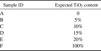
Figure 1(a) shows the transmittance spectra of the film at 200–1200 nm under varying doping concentrations. The impurity of Ti significantly alters the ultraviolet cutoff edge of the film. As the amount of Ti doping increases, the cutoff edge gradually moves from sample A to F. Figure 1(b) shows the refractive index (n) of all samples before and after heat treatment. Due to the higher refractive index of TiO2 compared to Ta2O5, the refractive index of samples A–F increases with the Ti content. Furthermore, there are notable differences in the refractive index of the samples before and after heat treatment. Sample F, which will be discussed in Section 2.2, is the only coating that undergoes a transition from an amorphous to a crystalline structure after heat treatment. The crystallization results in a higher density and a more ordered structure, leading to an increase in refractive index. In contrast, the other samples (A–E) remain amorphous, with a slight decrease in refractive index after annealing. This observation can be explained by the relationship between the refractive index and packing density, suggesting that annealing reduces the film’s packing density. These findings are consistent with the typically reported correlation between optical constants and annealing temperature[ Reference Lv, Huang, Zhang, Deng, Gong, Wang, Pan, Li and Jin 11 ].
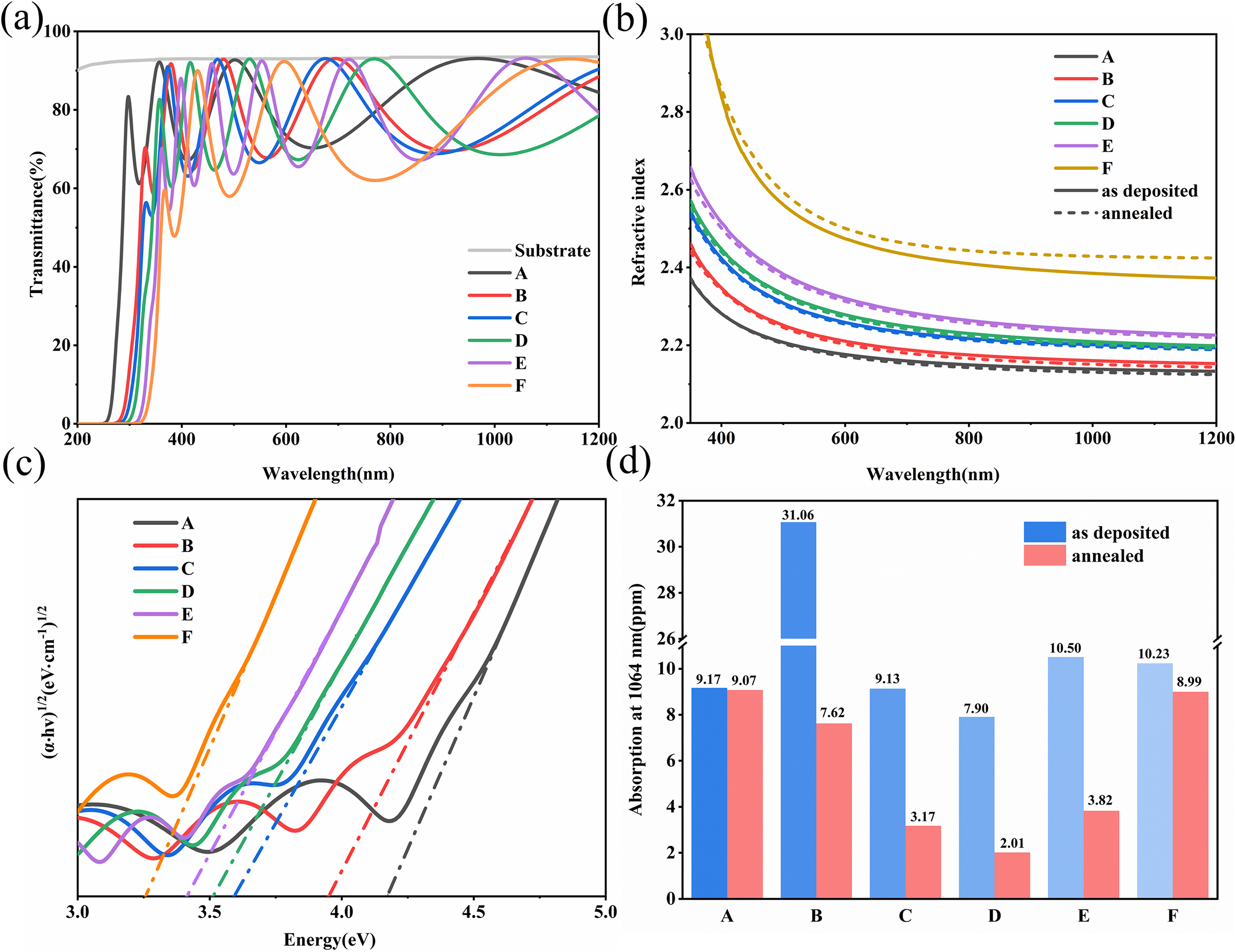
Figure 1 Optical properties of the films: (a) transmittance; (b) refractive index n; (c) band gap of unannealed samples; (d) absorption.
The optical band gap of the coating is estimated by the Tauc equation[ Reference Wen, Zhu, Chai, Liu, Shi, Du and Shao 16 ]. Figure 1(c) shows the band gap of the unannealed samples, with sample A having a band gap of 4.169 eV, and sample F having a band gap of 3.246 eV. The band gaps of the other doped samples decrease systematically with increasing doping concentration. According to Table S1 in the Supplementary Material, the band gaps of all coatings exhibit a slight increase after annealing. Thermal treatment in air may induce relaxation in the film, potentially adjusting its composition and reducing defect density, which could further lead to an increase in the bandgap. This will be further explained in Section 2.4.
Figure 1(d) shows the absorption of the film at 1064 nm. The value of unannealed films is represented in blue, while that of the annealed films is shown in red. For every identical sample, the red bar graph values are consistently lower than those of the blue bar graph, indicating that annealing effectively reduces the film’s absorption. For undoped samples A and F, the absorption decreased from 9.17 to 9.07 ppm and from 10.23 to 8.99 ppm after annealing, respectively. This suggests that the annealing process can only partially reduce the absorption of pure Ta2O5 and TiO2.
Doped, as-deposited films (B–E), except for sample D, exhibit absorption values that are almost equal to or exceed that of pure Ta2O5 (A), particularly sample B (5%), which shows an absorption of 31.06 ppm. This phenomenon may be attributed to the disorder among atoms within the microstructure of the mixed material, potentially caused by lattice distortion due to the addition of Ti, which increases defects in the film and consequently enhances absorption[ Reference Wen, Zhu, Chai, Liu, Shi, Du and Shao 16 ]. For the annealed samples, absorption initially decreases and then increases with rising doping concentrations, suggesting that this behavior may be related to the material composition; a detailed discussion is provided in Section 2.3 on the formation energy and composition. Among these samples, the one with a designed doping concentration of 15%, sample D, exhibits the lowest absorption after annealing, at 2.01 ppm.
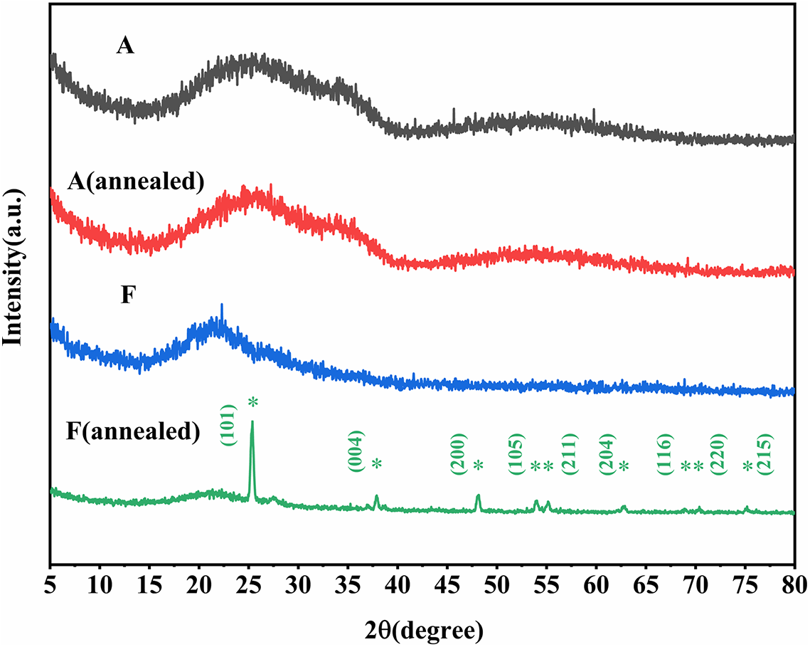
Figure 2 X-ray diffraction patterns of sample A (Ta2O5) and sample F (TiO2) before and after annealing.
2.2 Structural characterization
Figure 2 shows X-ray diffraction (XRD) images of samples A (pure Ta2O5) and F (pure TiO2) before and after heat treatment at 500°C. For sample A, there is minimal difference in the curves before and after annealing, with both curves appearing smooth and lacking distinct peaks, indicating an amorphous structure. In contrast, sample F shows a notable difference before and after annealing. Sample F before heat treatment is amorphous, and annealing causes the film to transform from amorphous to crystalline. The XRD spectrum shows obvious characteristic peaks of the anatase phase[ Reference Alhomoudi and Newaz 24 ]. Typically, amorphous Ta2O5 begins to exhibit a hexagonal phase at temperatures above 650°C[ Reference Lv, Huang, Zhang, Deng, Gong, Wang, Pan, Li and Jin 11 ], whereas TiO2 generally starts forming anatase crystals above 400°C. Thus, annealing at 500°C induces crystallization in sample F but has negligible impact on the structure of sample A. To further investigate the structural changes induced by doping and annealing, Raman spectroscopy was employed for additional analysis and characterization.
Figure 3 Raman analysis of the samples before and after annealing. (a) Raman spectra. The dark curve represents the unannealed sample, while the light curve corresponds to the annealed sample. Vertical lines indicate the diffraction peaks position of TiO2 anatase (gray lines) and rutile (black lines) phases. (b) First derivative of the normalized Raman spectra in the 550–750 cm–1 region. (c) The horizontal coordinates (Raman shift) and the absolute values of the vertical coordinates corresponding to the extremum points of the normalized Raman spectra slopes for samples A–E.
All samples were subjected to Raman spectroscopy analysis both before and after annealing process. To improve the analysis of peak positions, the data were smoothed using techniques similar to those reported in previous studies[ Reference Abernathy, Amato, Ananyeva, Angelova, Baloukas, Bassiri, Billingsley, Birney, Cagnoli, Canepa, Coulon, Degallaix, Di Michele, Fazio, Fejer, Forest, Gier, Granata, Gretarsson, Gretarsson, Gustafson, Hough, Irving, Lalande, Lévesque, Lussier, Markosyan, Martin, Martinu, Maynard, Menoni, Michel, Murray, Osthelder, Penn, Pinard, Prasai, Reid, Robie, Rowan, Sassolas, Schiettekatte, Shink, Tait, Teillon, Vajente, Ward and Yang 15 ]. In the spectra shown in Figure 3(a), as the film is transparent at 532 nm, the test spectrum will contain information about the fused quartz. By comparing the spectrum with that of the background fused silica, the spectral bands around 460, 605 and 800 cm–1 are attributed to the substrate rather than the film[ Reference Bergler, Cvecek, Werr, Brehl, De Ligny and Schmidt 25 ]. Specifically, the band at 460 cm–1 is associated with the Si-O-Si bond angle distribution (around 440 cm–1) and four-membered SiO4 defect rings (around 490 cm–1). The boundary between these two bands is not clearly defined, likely due to changes in the quartz surface ring structure caused by polishing and surface cleaning of the substrate. The band at 605 cm–1 is attributed to three-membered SiO4 defect rings, while the band at 800 cm–1 is assigned to Si-O stretching vibrations. For sample F with pure TiO2, the difference before and after annealing is as obvious as that in the XRD experiment. The bands at 240, 450, and 610 cm–1 of the film before annealing exhibit the characteristics of rutile phase. Considering their broadening (higher than 30 cm–1), it can be concluded that the unannealed sample F is amorphous, with a poorly crystalline rutile structure present[ Reference Boukrouh, Bensaha, Bourgeois, Finot and Marco de Lucas 26 ]. After annealing, the characteristic bands at 144, 400, 520 and 642 cm–1 indicate the formation of a distinct anatase structure in sample F[ Reference Alhomoudi and Newaz 24 ]. Notably, the band at 144 cm–1 corresponds to the first Raman active mode (Eg) of anatase, associated with the symmetric stretching vibration of the O-Ti-O bond. In addition, the band at 400 cm–1 is attributed to the symmetric bending vibration of the O-Ti-O bond. The higher peak intensity and narrower peak broadening indicate that it has a high crystallinity, which is consistent with the XRD test results.
Based on the peak widths of the spectral bands for samples A–E, it can be concluded that all of them exhibit an amorphous structure[ Reference Joseph, Bourson and Fontana 27 ]. Since the primary component is Ta2O5, their spectral features are similar. After excluding the influence of the quartz glass substrate, the contributions of the thin films in the Raman spectra mainly appear in the ranges of 100–300 and 550–750 cm–1. For sample A (Ta2O5), the spectral features display typical characteristics of amorphous Ta2O5. After annealing, the mode around 240 cm–1 suggests that some crystallization has occurred within the amorphous structure[ Reference Joseph, Bourson and Fontana 27 , Reference Chen, Feng, Fan, Han, Li and Lai 28 ]. The modes in the 100–300 cm–1 range primarily arise from the bending vibrations of the O-Ta-O bonds in the TaO6 octahedron[ Reference Meng, Rai, Katiyar and Bhalla 29 ]. This mode is highly sensitive to the Ti content. Even though Ta2O5 is the main material, the mode shifts to lower frequencies and its intensity increases with increasing Ti content. Sample B (5%), with a low Ti content, retains the spectral characteristics of Ta2O5. In sample C (10%), the mode at around 200 cm–1 cannot be independently assigned to Ta2O5 or TiO2, suggesting that coupling between the O-Ta-O and O-Ti-O vibrations has occurred. For samples D (15%) and E (20%), the corresponding modes appear at 144 and 130 cm–1, respectively. These modes are closer to those observed in annealed sample F (TiO2), indicating similarities to the rutile phase. The spectral bands in the 550–750 cm–1 range are attributed to the stretching vibrations of Ta-O bonds in TaO6 [ Reference Chen, Feng, Fan, Han, Li and Lai 28 ]. The variation in this region with Ti content is relatively less pronounced. Since sample F (pure TiO2) exhibits a similar mode in the 600–650 cm–1 range before and after annealing, it can be inferred that the growth of the mode around 620 cm–1 in the Ti-doped Ta2O5 samples is due to the increased Ti content.
We aim to derive information about the film relaxation state from the peak broadening, which reflects the degree of ordering within the film. Roorda et al. [ Reference Roorda, Sinke, Poate, Jacobson and Fuoss 30 ] reported a correlation between structural relaxation and the linewidth of Raman peaks, where a reduction in bond angle distribution leads to the sharpening of Raman peaks. In this study, the main Raman contribution regions are between 100 and 300 cm–1 as well as 550 and 750 cm–1. The former region shows larger shifts in peak positions with doping, and is interfered with by the substrate peak at around 70 cm–1. Therefore, we focus on the latter region to assess the relaxation state of the films. Abernathy et al. [ Reference Abernathy, Amato, Ananyeva, Angelova, Baloukas, Bassiri, Billingsley, Birney, Cagnoli, Canepa, Coulon, Degallaix, Di Michele, Fazio, Fejer, Forest, Gier, Granata, Gretarsson, Gretarsson, Gustafson, Hough, Irving, Lalande, Lévesque, Lussier, Markosyan, Martin, Martinu, Maynard, Menoni, Michel, Murray, Osthelder, Penn, Pinard, Prasai, Reid, Robie, Rowan, Sassolas, Schiettekatte, Shink, Tait, Teillon, Vajente, Ward and Yang 15 ] demonstrated that the absolute value of the maximum slope can reflect the linewidth of Raman peaks composed of Lorentzian or Gaussian functions. A larger slope corresponds to a narrower peak, indicating better relaxation. We adopted a similar method by normalizing the 550–750 cm–1 range (Figure S1 in the Supplementary Material) and taking the first derivative, as shown in Figure 3(b). To provide a clearer visual representation, the changes in the coordinates of the slope minima for samples A–E before and after annealing are illustrated in Figure 3(c). The upper panel shows the changes in the horizontal coordinates (Raman shift) corresponding to the extremum points before and after annealing. For samples with TiO2 content greater than or equal to 10% (C–E), the Raman shifts move toward higher frequencies after annealing, indicating that the incorporation of Ti modifies the internal microstructure of the films, resulting in additional changes during thermal treatment compared to samples A and B. The lower panel displays the changes in the absolute values of the vertical coordinates (|first derivative| ) corresponding to the extremum points before and after annealing. As previously mentioned, larger |first derivatives| correspond to narrower peak widths. For most samples, except sample D, the values increase after annealing, suggesting that the annealing process narrows the Raman peaks, leading to a more relaxed material. Furthermore, the gradual decrease in the |first derivative| with increasing Ti content implies a broadening of the peak width for this spectral band, indicating that the addition of Ti may, to some extent, reduce the structural relaxation.
2.3 Formation energy and composition
X-ray photoelectron spectroscopy (XPS) was utilized to observe the characteristic peaks of a series of doped films, with the peaks of the main elements being fitted for analysis. Figures 4 and Figure S2 (Supplementary Material) present the XPS analysis of all samples before and after annealing, respectively, illustrating the chemical composition and electronic structure of the samples. According to existing research, the binding energy of Ta 4f7/2 for Ta5+ in Ta2O5 is typically in the range of 26.0–26.4 eV[ Reference Simpson, White, Watts and Baker 31 ]. In addition, the binding energies for Ta-O and Ti-O bonds are approximately 530.5 eV, and the binding energy of Ti 2p3/2 is around 458.6 eV[ Reference Wen, Zhu, Chai, Liu, Shi, Du and Shao 16 ]. Table 2 summarizes the peak information for Ta, while the data for O and Ti are detailed in Table S2 in the Supplementary Material. The results indicate that the characteristic peaks of samples A and F with amorphous structures exhibit lower binding energies than these standard values. Notably, only sample F after annealing, which exhibits an anatase structure, shows a Ti 2p3/2 binding energy close to the standard value (458.63 eV). Therefore, the possible reason for the decrease in the binding energy mentioned above is that the amorphous structure of the film has a smaller binding energy than the standard crystal[ Reference Aswal, Muthe, Tawde, Chodhury and Yakhmi 32 ].

Figure 4 Typical XPS spectra of unannealed films: (a) Ta 4f; (b) O 1s (OI refers to lattice oxygen, OII corresponds to hydroxyl groups and OIII represents surface-adsorbed oxygen); (c) Ti 2p.
Table 2 Fitting results of the Ta 4f7/2 peak for the films.
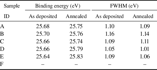
Figure 4(a) illustrates that the typical Ta 4f spectra in all Ta-containing coatings (samples A–E) display doublets (Ta 4f5/2 and Ta 4f7/2), corresponding to spin-orbit splitting, with a splitting energy of approximately 1.9 eV and an area ratio of about 3:4[ Reference Simpson, White, Watts and Baker 31 ]. Table 2 shows that after heat treatment, the Ta 4f7/2 peak shifts to higher binding energies in all samples. For the as-deposited Ti-doped samples, the position of the Ta 4f7/2 peak tends to decrease progressively with increasing Ti content. Existing reports have indicated that the direction of the Ta 4f peak shift is related to the electronegativity of the doping elements; since the electronegativity of Ti is lower than that of Ta, the peak position shifts to lower energies[ Reference Wen, Zhu, Chai, Liu, Shi, Du and Shao 16 ]. The full width at half maximum (FWHM) of the characteristic peak can often reflect the concentration of different valence states in the material[ Reference Banerjee, Hamnabard and Joo 33 ]. Except for sample C, the FWHM of the Ta 4f7/2 characteristic peak decreases in all Ta-containing samples after annealing compared to before annealing. This suggests that, in addition to Ta5+, the samples also contain a small amount of Ta4+, and that annealing can decrease the Ta4+ and increase the Ta5+ content. Before annealing, the FWHM of Ta 4f7/2 follows the order D < C = E < A < B, whereas after annealing, the order changes to D < E < A < C < B. Notably, the FWHM of samples D and E remains consistently smaller than that of sample A, indicating that higher concentrations of Ti doping can lead to a higher Ta5+ content in the films compared to pure Ta2O5 film.
Figure 4(b) presents a typical XPS spectrum of O 1s in the films. The OI peak is considered to correspond to lattice oxygen within the oxide, while the OII and OIII peaks are generally attributed to oxygen in surface contaminants such as hydroxyl groups, adsorbed water and carbonates[ Reference Ramos-Moore, Ferrari, Diaz-Droguett, Lederman and Evans 34 ]. Table S2 also provides the specific peak positions of O (lattice oxygen). For most samples, thermal treatment leads to an increase in the binding energy of lattice oxygen. In samples B–E, the binding energy of O before heat treatment decreases progressively with increasing doping concentration. This change is attributed to the introduction of Ti doping, which creates holes and captures some electrons, thereby reducing the electron density of O and leading to a decrease in binding energy[ Reference Pazhanivelu, Paul Blessington Selvadurai, Murugaraj, Panneer Muthuselvam, Chou and Mater 35 ].
In all Ti-containing coatings (B–F), the Ti 2p peaks can be fitted into two sub-peaks: Ti 2p1/2 and Ti 2p3/2. The splitting energy between these sub-peaks is approximately 5.8 eV, with an area ratio of about 1:2[ Reference Wen, Zhu, Chai, Liu, Shi, Du and Shao 16 ]. Figure 4(c) shows the presence of the Ta 4p1/2 peak at the position of the Ti 2p characteristic peak. Therefore, during peak fitting of all Ti-doped samples, the Ta 4p1/2 peak is identified and marked. As the Ti doping level increases, the relative intensity of the Ta 4p1/2 peak decreases, which is consistent with the observed trend in the expected Ta/Ti ratio.
The elemental composition of each coating before and after annealing was determined by XPS, and the resulting elemental and mass ratios are presented in Table 3. In this table, ‘XPS (Ta:Ti:O)’ represents the elemental ratios obtained through peak fitting of the XPS spectra, while ‘Measured TiO2 content’ represents the percentage of TiO2 in the total mass, derived from the elemental ratios. This value can be used for comparison with the data presented in Table 1. Although these measured ratios differ slightly from the expected mass ratios of the coatings, the variations among different doping levels are relatively pronounced. The slight changes in the relative content of Ta and Ti before and after annealing may be attributed to differences in the test locations, and these variations are within the acceptable range.
Table 3 Elemental composition of the films and the calculated mass ratio of TiO2.
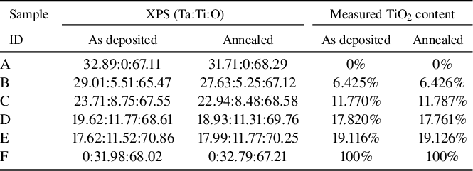
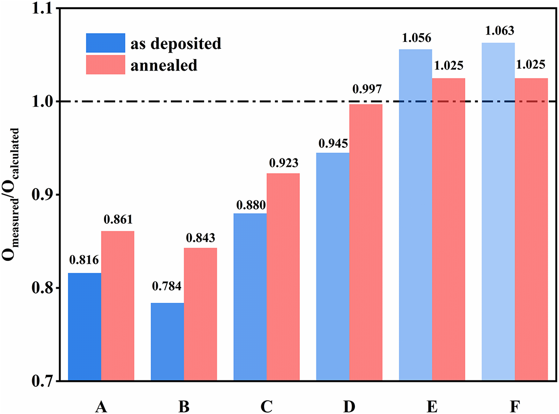
Figure 5 The ratio of O measured (measured oxygen content) to O calculated (calculated stoichiometric oxygen content) in the films.
Figure 5 illustrates the comparison of oxygen content in all samples before and after annealing. Here, O measured represents the actual oxygen content measured experimentally, whereas O calculated refers to the oxygen content calculated based on the complete oxidation of Ta and Ti present in the tested films. The closer the ratio of O measured/O calculated is to 1.0, the closer the actual oxygen content of the coating is to the standard stoichiometric ratio. The experimental results indicate that the O measured/O calculated ratio for Ta-containing samples is less than 1.0, suggesting an oxygen deficiency. In contrast, for sample F (TiO2), this ratio is greater than 1.0, indicating an excess of oxygen, similar to the situation of oxygen excess in TiO2 reported in the literature[ Reference Andres, Toledano-Luque, Prado, Navacerrada, Martil, Gonzalez-Diaz, Bohne, Rohrich and Strub 36 ]. The ratio of all coatings approaches 1.0 after annealing, suggesting that annealing is an effective method for achieving an ideal stoichiometric ratio. However, for samples A and F, the ratios post annealing only reach 0.861 and 1.025, respectively. To get closer to the standard stoichiometric ratio, doping is needed. The annealed films exhibit a relatively distinct pattern. For sample D, the O measured/O calculated ratio is 0.997, which is the closest to 1.0. When the Ti content is below this doping level, the film exhibits an oxygen-deficient state, whereas a higher Ti content results in over-oxygenation.
This trend is consistent with the absorption of the films in Figure 1(d). For sample A, the ratio of O measured/O calculated increases from 0.816 to 0.861, with absorption values of 9.17 ppm before annealing and 9.07 ppm after. This increase in the ratio corresponds to a decrease in absorption; however, since the ratio does not approach 1.0, the absorption value remains relatively high. Before annealing, the absorption of sample B is as high as 31.06 ppm. The stoichiometric ratio of the film is Ta:Ti:O = 29.01:5.51:65.47, with the ratio O measured/O calculated = 0.784, indicating that the film is in an oxygen-deficient state, which represents the largest deviation from the ideal stoichiometry. After annealing, the ratio increased to 0.843, indicating a rise in oxygen content, while the absorption decreased to 7.62 ppm. In addition, the annealed sample D exhibits the lowest absorption of 2.01 ppm. At this doping level, the film’s O measured/O calculated ratio is 0.997, indicating a composition that is closest to the stoichiometric ratio expected for fully oxidized Ta and Ti. For sample E, the film exhibits an O measured/O calculated ratio of 1.056 before annealing, with an absorption of 10.50 ppm, indicating an over-oxidized state. After annealing, the ratio decreases to 1.025 and the absorption reduces to 3.82 ppm. This suggests that annealing can improve the oxygen deficiency and excess in the film, bringing its chemical composition closer to the ideal stoichiometric ratio, thereby achieving lower absorption values. In general, these observations are consistent with the trend that the closer the Ta and Ti in the film are to being fully oxidized, the lower the absorption.
Based on the above experimental results, we speculate that absorption is related to the chemical composition of the film. After annealing, absorption decreased to varying degrees, indicating that heat treatment in an air atmosphere would make the film closer to the ideal stoichiometric ratio; for undoped films, annealing had limited effect on the reduction of absorption, indicating that it is difficult to achieve full oxidation of thin film materials with pure Ta2O5 and TiO2 simply by heat treatment, and by doping with Ti, the composition of the coating after annealing can be closer to the standard stoichiometry, thereby further reducing the absorption; however, under fixed heat treatment conditions, there is an optimal range for TiO2 content, and absorption will increase if it is lower or higher than this range. The following will explain the influence of components on the absorption of thin films through theoretical simulations.
2.4 Theoretical calculation and analysis of Ti-doped Ta2O5
In order to explain the optimal range of Ti doping from a mechanistic perspective and why the absorption is lower within this range, Ti-doped amorphous Ta2O5 models were established. To ensure the validity of the initial model, we first plotted the pair distribution function (PDF) based on the amorphous Ta2O5 structure obtained from ab initio molecular dynamics (AIMD) simulations, as shown in Figure 6. The plot confirms that the structure is indeed amorphous, which is consistent with previous reports[ Reference Damart, Coillet, Tanguy and Rodney 37 ]. The first peak of the PDF for the Ta-O bond is observed at 1.93 Å, for the O-O bond at 2.83 Å and for the Ta-Ta bond at 3.76 Å. The peak values fall within the range reported in experimental studies: 1.92–1.99 Å for the Ta-O bond and 3.14–3.88 Å for the Ta-Ta bond[ Reference Bassiri, Liou, Abernathy, Lin, Kim, Mehta, Shyam, Byer, Gustafson, Hart, MacLaren, Martin, Route, Rowan, Stebbins and Fejer 38 ].

Figure 6 Pair distribution function of the simulated amorphous Ta2O5 model.
Based on the experimental observations, we introduced two types of defects into the theoretical model. XPS analysis of sample A revealed the presence of oxygen vacancies in the Ta2O5 film, which we simulated by removing oxygen atoms. For the introduction of titanium, we chose to substitute Ti atoms for Ta atoms. During the dual-source co-evaporation process, Ti atoms occupy a fraction of the deposition sites originally intended for Ta atoms. Upon oxidation, Ti atoms bond with oxygen, replacing the regions where Ta-O polyhedra would have formed with Ti-O polyhedra. Considering that octahedral coordination of TaO6 is predominant in amorphous Ta2O5 [ Reference Damart, Coillet, Tanguy and Rodney 37 ], and the small voids in the structure lead to high defect formation energies for Ti atoms in interstitial sites, substitution sites are chosen. By removing one O atom from the amorphous Ta2O5 structure and replacing one, two and three Ta atoms with an equivalent number of Ti atoms, we developed three doped models: 1VO+1TiTa, 1VO+2TiTa and 1VO+3TiTa. After structural relaxation, the lattice vector changes, as shown in Figure S3 in the Supplementary Material, and there is no significant structural migration.
To further investigate the contribution of elemental composition to the impurity energy levels within the bandgap of the Ti:Ta2O5 model, the DFT method was used to calculate the partial density of states (PDOS), with the zero-energy level set at the top of the valence band, as shown in Figure 7. For the pure amorphous Ta2O5 model, the calculated bandgap is 4.43 eV, which is slightly higher than the previously reported experimental values of 3.8–4.3 eV[ Reference Hur 39 ]. As shown in Figure 7(a), there is strong hybridization between the O 2p and Ta 5d orbitals in the valence band, resulting in a bandwidth of approximately 6.5 eV, which is consistent with previously reported theoretical calculations[ Reference Guo and Robertson 9 ]. The top of the valence band is primarily contributed by the O 2p orbitals, while the bottom of the conduction band is mainly composed of contributions from the Ta 5d orbitals. In crystalline structures, the crystal field effect of the TaO6 octahedra typically causes energy level splitting of the Ta 5d orbitals in the conduction band. However, due to the inherent disorder in the amorphous structure, the Ta 5d orbitals in the conduction band of this study’s model do not split into the t2g (3d xy , 3d xz and 3d yz ) and eg (3d x 2 -y 2 and 3d z 2 ) orbitals as they do in crystalline structures[ Reference Zhou, Li and Guo 40 ].
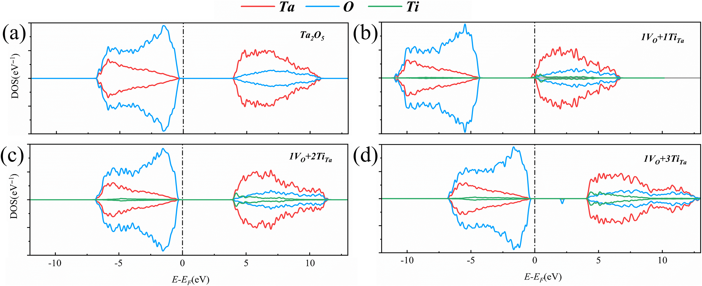
Figure 7 Theoretically calculated density of states: (a) Ta2O5; (b) 1VO+1TiTa; (c) 1VO+2TiTa; (d) 1VO+3TiTa. VO represents an oxygen vacancy, which involves the removal of an oxygen atom. TiTa refers to the replacement of tantalum with titanium.
For the doping models, previous studies have reported that when an O vacancy is created, electrons that have not formed stable chemical bonds may interact with nearby Ta atoms to form weakly bound states such as dangling bonds, due to the Coulomb effect[ Reference Guo and Robertson 9 ]. Since the energy associated with these states is higher than that of covalent bond formation, a donor energy level is introduced near the bottom of the conduction band above the valence band. Similarly, considering some cases of p-type doping[ Reference Xia, Shao, He, Wang, Wu, Jiang, Duhm, Zhao, Lee and Jie 41 ], we hypothesize that when Ti atoms are substituted at Ta sites in the model, Ti provides fewer electrons to the surrounding environment compared to Ta, leading to the formation of holes on nearby oxygen atoms and the establishment of acceptor energy levels. When both types of doping are present, electrons from the donor energy levels preferentially occupy the acceptor energy levels. This phenomenon is known as ‘impurity compensation’[ Reference Zhou, Li and Guo 40 ].
For a structure containing one O vacancy and one Ti impurity, denoted as 1VO+1TiTa, as shown in Figure 7(b), the impurity energy level corresponds to the Ta 5d orbital, located 0.47 eV above the bottom of the conduction band. The PDOS is similar to those of previously reported oxygen vacancy defects, with the donor energy level just below the conduction band also associated with the Ta 5d orbital. From the perspective of impurity compensation, the presence of VO is in excess, and the acceptor energy level introduced by TiTa doping cannot fully accommodate all the donor charges from VO. Therefore, this type of defect is similar to oxygen vacancy.
In the 1VO+2TiTa structure, Figure 7(c) shows that the top of the valence band is primarily composed of O 2p orbitals, while the bottom of the conduction band comprises contributions from both Ta 5d and Ti 3d orbitals. The electrons from the donor energy level generated by the oxygen vacancy are exactly compensated by the acceptor energy levels introduced by the TiTa dopants. As a result, all electrons participate in the formation of stable chemical bonds, leaving no unoccupied states in the bandgap. Figure 8 illustrates the differential charge distribution for the 1VO+2TiTa structure, with Ta atoms represented in gold, O atoms in red and Ti atoms in blue. The blue electron cloud indicates regions of electron loss, while the yellow regions denote areas of electron gain. The differential charge analysis reveals that electron loss primarily occurs at Ta atoms adjacent to the O vacancy, while electron gain is predominantly concentrated on the two Ti atoms and the nearby O atoms. The coexistence of VO and TiTa results in electron transfer from Ta to Ti within the system. As previously mentioned, the positively charged centers formed by Ta at oxygen vacancies interact with electrons to create dangling bonds, which are weaker than stable chemical bonds. When Ti replaces Ta, it generates holes in the surrounding structure. These holes attract nearby electrons, particularly those forming weak bonds with Ta, leading to observable electron loss at Ta sites and electron gain at Ti sites. The bandgap of the 1VO+2TiTa structure is calculated to be 4.40 eV, which is slightly smaller than that of the pure Ta2O5 model.
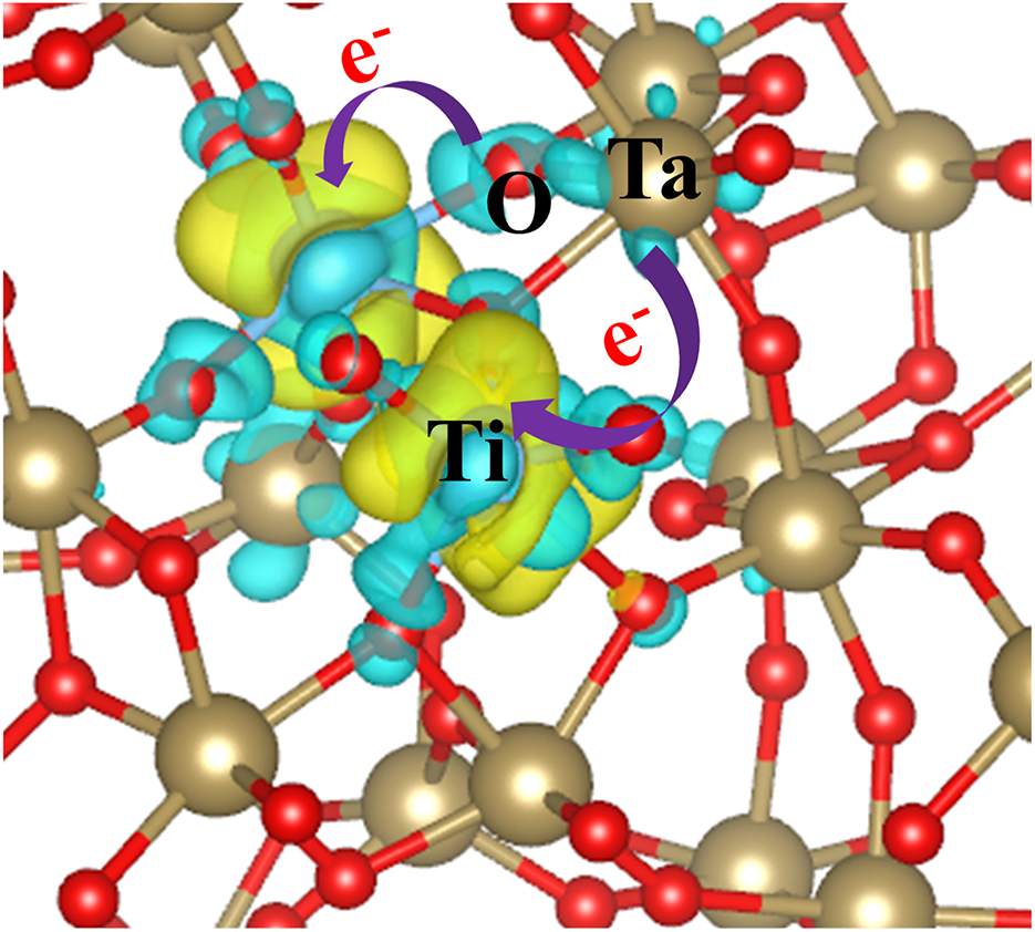
Figure 8 Differential charge distribution around Ti atoms in the 1VO +2TiTa model. The gold sphere represents a tantalum atom, the blue sphere represents a titanium atom and the red sphere represents an oxygen atom. The blue electron cloud indicates a loss of electrons, while the yellow cloud represents a gain of electrons.
When a 1VO+3TiTa configuration is introduced into the system, Figure 7(d) illustrates the formation of an acceptor energy level just above the valence band, with the acceptor state being predominantly composed of O 2p orbitals, located 1.79 eV above the valence band maximum. In this model, the TiTa concentration is excessive, and the electrons from the donor energy level associated with the O vacancy do not fully compensate for the holes generated by the Ti atom. As a result, the system exhibits characteristics typical of acceptor doping.
The impurity energy levels within the energy band significantly influence the photoelectric properties of the system. Under the influence of external light and heat, electrons in the donor energy level can be readily excited into the conduction band, and electrons in the valence band can similarly be excited into the unoccupied acceptor energy levels. These processes result in increased absorption by the material, leading to an undesirable increase in absorption. The perspective can also be confirmed by the calculated extinction coefficient. Figure 9 presents the extinction coefficient curves of the four models as a function of energy. The absorption region for the 1VO+1TiTa model is observed between 1 and 3 eV, while the 1VO+3TiTa model shows absorption above approximately 2 eV. In contrast, the extinction curves for Ta2O5 and 1VO+2TiTa exhibit no peaks within the 0–4 eV range.
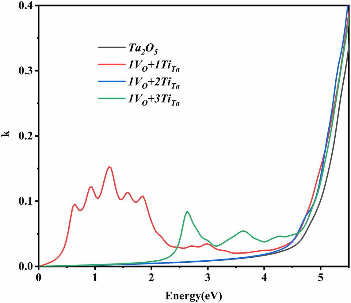
Figure 9 Theoretically calculated extinction coefficient k.
Thus, to obtain low-absorption materials, the compositions corresponding to Ta2O5 and 1VO+2TiTa are relatively ideal. However, producing a Ta2O5 coating without oxygen vacancies through conventional heat treatment processes poses significant challenges. We aim to achieve a coating with the target composition of 1VO+2TiTa through controlled doping and annealing. Based on the experimental results, it can be concluded that 1VO+1TiTa corresponds to samples B and C, 1VO+2TiTa corresponds to sample D and 1VO+3TiTa corresponds to sample E. This also explains that as the doping concentration increases, the absorption of annealed samples first decreases and then increases. Outside the appropriate range, an excess or deficiency of Ti introduces extra charges into the film, leading to increased absorption.
In summary, both experimental and theoretical evidence demonstrate that composition is the primary factor influencing thin film absorption, while the deposition method typically affects the film’s density and structure. Therefore, we conclude that, with proper control of composition, low-absorption films can still be fabricated using ion beam-assisted electron-beam evaporation, even without employing IBS.
2.5 Preparation of high-reflectivity film
Based on the process of sample D, which exhibited the lowest absorption, we used it as the high-refractive-index layer (H) to fabricate the high-reflectivity layer. SiO2, a material with very low absorption, was used for the low-refractive-index layer (L), and the multilayer structure followed the design substrate/(HL)17/air, with quarter-wave (QW) optical thicknesses at 1064 nm. The multilayer film underwent the same heat treatment as the single-layer films. The transmission curve of the high-reflectivity film is shown in Figure 10, demonstrating high reflectivity across the 950–1130 nm wavelength range. The absorption at 1064 nm was measured before and after annealing, showing a reduction from 66.39 to 1.70 ppm after heat treatment. Most ultra-low-absorption thin films are currently fabricated using IBS. In this experiment, it is demonstrated that by combining compositional control with annealing processes, ultra-low-absorption thin films can be achieved through ion beam-assisted electron-beam evaporation.
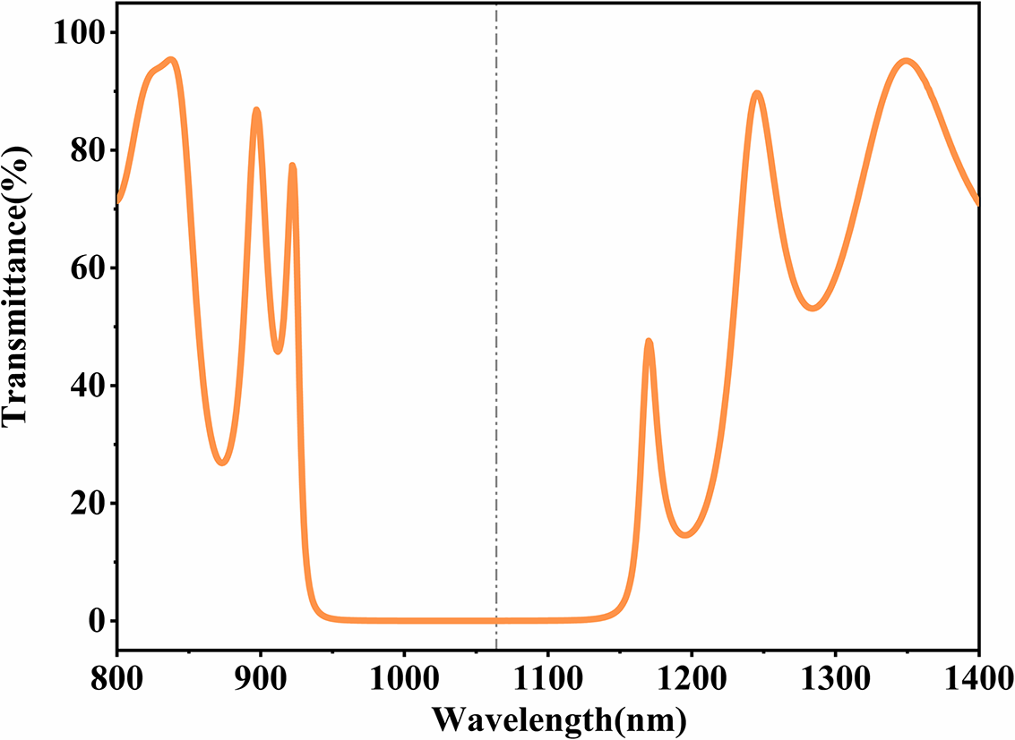
Figure 10 Measurement of transmittance spectrum of high-reflectivity film.
3 Discussion
Single-layer and multilayer Ta2O5 films with varying Ti concentrations were fabricated using ion beam-assisted electron-beam evaporation and annealed at 500°C. The experimental results show that all films are amorphous before heat treatment. Compared to structural factors, the composition appears to have a more significant impact on absorption. Amorphous films with compositions closer to the fully oxidized states of Ta and Ti exhibit lower absorption. From a structural perspective, TiO2 significantly alters the Raman response of the films and appears to increase structural disorder. In contrast, annealing tends to relax the structure of films. From a compositional standpoint, both doping and annealing contribute to bringing the films closer to the ideal stoichiometric ratio. However, relying solely on one of them has limitations. A combination of doping and annealing is required to achieve the optimal condition, corresponding to ultra-low absorption. Theoretical calculations reveal the charge transfer associated with the introduction of Ti, which ‘neutralizes’ oxygen vacancies, and explain that there is an optimal concentration range for Ti. When the actual content of TiO2 is around 17.8%, the absorption of the single-layer film at 1064 nm can be reduced to 2.01 ppm after annealing, and the absorption of the high-reflectivity film prepared using this process reached 1.70 ppm after annealing. This implies that, with the correct composition, low-absorption films can be fabricated even without the need for high-cost deposition methods such as IBS. This study provides theoretical and technical insights for the lower-cost, faster fabrication of ultra-low-absorption films.
4 Methodology
4.1 Experimental methods
A series of thin films were experimentally deposited on fused silica substrates (Φ25.4 mm × 2.5 mm) using an ion beam-assisted electron-beam co-evaporation process under O2/Ar atmospheric conditions. The substrates were subjected to super-polishing, followed by ultrasonic cleaning and thorough rinsing with deionized water (18.2 MΩ·cm). The baseline vacuum level was maintained at 1.0 × 10⁻⁴ Pa, and the deposition temperature was set to 250°C. The materials used for the film deposition were Ta with a purity of 99.99% and Ti3O5 particles, with a particle size ranging from 1 to 3 mm and a purity of 99.99%. During the evaporation process, the substrates were positioned on the sample holder above the electron-beam evaporation system. The oxygen ion beam generated by the radio frequency (RF) ion source bombards the surface of the film, enhancing the oxidation of the coating while simultaneously assisting in the deposition process, resulting in a denser film structure. The voltage applied to the auxiliary ion source is 1100 V, with a current of 1000 mA.
Pre-experiments were conducted prior to doping. Based on the relationship between the deposition rates of Ta2O5 and TiO2 single layers and the beam current, single-layer films with different doping ratios were prepared by pre-set Ta and Ti deposition beam current according to the designed doping film composition. The actual doping composition of these single layers was characterized using XPS, which allowed for the determination of the beam currents for each component during the preparation of layers with different doping ratios. Subsequently, deposition time was controlled to fabricate doped single layers of varying thicknesses. The optical thickness of these doped layers was obtained through transmission spectral fitting, establishing a relationship between optical thickness and deposition time under the specified process parameters. Finally, during the deposition of multilayer films, the layer thickness was controlled by adjusting the deposition time. In the process of preparing high-reflectivity films, the deposition rate for Ti:Ta2O5 was 2 Å/s, and that for SiO2 was 6 Å/s. Throughout the entire process, the crystal monitor was only employed as an auxiliary tool during the deposition of pure TiO2 and Ta2O5 single layers. The deposited samples underwent an annealing process, with the temperature increased at a rate of 100°C/h from room temperature to 300°C, held at 300°C for 8 h, and then ramped up to 500°C at a rate of 50°C/h. After reaching 500°C, the temperature was maintained for 10 h, followed by cooling to 350°C at 50°C/h. Finally, the samples were allowed to cool naturally to room temperature. The entire heat treatment process was conducted in a muffle furnace.
The transmittance of the samples in the wavelength range of 200–2500 nm was measured using a Cary 5000 ultraviolet-visible-near-infrared (UV-Vis-NIR) spectrophotometer, with a measurement accuracy of ±0.06%. The refractive index (n) and optical band gap of the films were estimated using the transmittance spectrum method and the Tauc equation, respectively[
Reference Ashraf, Waseem, Qureshi, Yunus, Aamir, Ullah and Saleem
42
,
Reference Galy, Marszewski, King, Feng, Yan and Tolbert
43
]. The absorption of the samples at 1064 nm was measured using laser-induced deflection (LID) technology, with single-point testing performed using a continuous laser[
Reference Mühlig, Kufert, Bublitz and Speck
44
]. The structure of the coating was characterized using an Empyrean X-ray diffractometer, with measurements taken at a grazing incidence angle of 0.5°. Raman scattering was analyzed using a LabRAM Odyssey spectrometer with a 532 nm laser. The binding energies of Ta, O and Ti in the films were determined by XPS using a monochromatic Al K $\unicode{x3b1}$
source (1486.6 eV) on a Thermo ESCALAB 250Xi instrument. Charge correction was applied using the C 1s standard peak at 284.8 eV, and the obtained spectra were fitted using peak deconvolution techniques[
Reference Jain, Biesinger and Linford
45
].
$\unicode{x3b1}$
source (1486.6 eV) on a Thermo ESCALAB 250Xi instrument. Charge correction was applied using the C 1s standard peak at 284.8 eV, and the obtained spectra were fitted using peak deconvolution techniques[
Reference Jain, Biesinger and Linford
45
].
4.2 Computational methods
The simulation calculation of Ta2O5 and Ti:Ta2O5 was implemented based on DFT using Vienna Ab initio Simulation Package (VASP) software [ Reference Kresse and Furthmüller 46 ]. Ta, O and Ti used the projector augmented wave (PAW) potentials Ta_pv, O and Ti_sv to treat the electron and ion interactions, and the spin polarization calculation was performed. Considering that real thin films are often disordered, we employed AIMD to model the amorphous structure of the Ta2O5 lattice[ Reference Joseph, Bourson and Fontana 27 ]. The calculation used the Perdew–Burke–Ernzerhof (PBE) generalized gradient approximation (GGA) to describe the exchange-correlation function[ Reference Perdew, Burke and Ernzerhof 47 ], and the electronic structure iteration convergence threshold was set to 10–6 eV. The orthorhombic phase λ-Ta2O5 proposed by Lee et al. [ Reference Lee, Kim, Kim, Kim and Park 48 ] was used as the primitive cell, with lattice constants of a = 6.25 Å, b = 7.40 Å and c = 7.66 Å. A 2×2×2 supercell containing 32 Ta atoms and 80 O atoms was created. According to the research of Pedersen et al. [ Reference Pedersen, Chang, Li, Pryds and Lastra 49 ], we enlarged the lattice vector of the supercell by a factor of 1.06 to make it more consistent with the experimental value of the density of amorphous Ta2O5. The supercell was subjected to a melt-and-quench procedure in the NVT ensemble using a Nosé–Hoover thermostat: 10 ps equilibration at 4000 K, then quenched at 1000 K below the theoretical melting point; the cooling process lasted 20 ps and equilibration for 20 ps at 1000 K. The AIMD simulation used a low-precision setting with a cutoff energy of 200 eV, a 1×1×2 k-point sampling and a time step of 2 fs[ Reference Bassiri, Borisenko, Cockayne, Hough, MacLaren and Rowan 50 ].
The ion positions and lattice vectors of the established Ta2O5 structure are structurally optimized by the PBEsol function, which provides better structural properties for the solid. The Brillouin zone was sampled with a 1×1×2 k-point grid for structural relaxation[ Reference Perdew, Ruzsinszky, Csonka, Vydrov, Scuseria, Constantin, Zhou and Burke 51 ]. The atomic force converges to within 0.02 eV/Å, and the cutoff energy is increased to 520 eV. The average density of the final Ta2O5 is 7.606 g/cm3, which is within the experimental value range (6.88–7.68 g/cm3)[ Reference Damart, Coillet, Tanguy and Rodney 37 ]. The k-point sampling of the static self-consistent is increased to 2×2×4. High-precision calculations of the obtained structures were performed using the Heyd–Scuseria–Ernzerhof (HSE06) hybrid functional to obtain accurate electronic structures[ Reference Heyd, Scuseria and Ernzerhof 52 ]. Due to their high computational requirements, these calculations only used a 1×1×2 k-point sampling. Different electron state densities can cause different dielectric responses.
The dielectric function
$\varepsilon ={\varepsilon}_1\left(\omega \right)+i{\varepsilon}_2\left(\omega \right)$
is an important function for describing optical properties. The imaginary part ${\varepsilon}_2\left(\omega \right)$
is a collection of optical properties and can be described as follows:
${\varepsilon}_2\left(\omega \right)$
is a collection of optical properties and can be described as follows:
 $$\begin{align}{\varepsilon}_2\left(\omega \right)=\frac{2{e}^2\pi }{\varOmega {\varepsilon}_0}{\sum}_{k,v,c} \mid {\psi}_k^c \mid \hat{u}\times r\;{\left|\;{\psi}_k^v\right|}^2\delta \left({E}_k^c-{E}_k^v-E\right),\end{align}$$
where
$\varOmega$
is the unit cell volume, v and c represent the valence band and conduction band, respectively, k represents the k-point, ω is the incident light frequency and $\hat{u}$
is the vector defining the polarization direction of the incident light field, which is considered to be an isotropic average value in the case of polycrystalline. The real part
$\hat{u}$
is the vector defining the polarization direction of the incident light field, which is considered to be an isotropic average value in the case of polycrystalline. The real part ${\varepsilon}_1\left(\omega \right)$
is obtained by the Kramers–Kronig relation[
Reference Lawal, Shaari, Ahmed and Jarkoni
53
]:
${\varepsilon}_1\left(\omega \right)$
is obtained by the Kramers–Kronig relation[
Reference Lawal, Shaari, Ahmed and Jarkoni
53
]:
 $$\begin{align}{\varepsilon}_1\left(\omega \right) = 1+\frac{2}{\pi}{p}{\int}_0^{\infty}\frac{\omega^{\prime }{\varepsilon}_2\left({\omega}^{\prime}\right)}{{\omega^{\prime}}^2-{\omega}^2}\mathrm{d}{\omega}^{\prime }.\end{align}$$
In the formula, p represents the principal value of the integral. The extinction coefficient k(ω) can be calculated using the following formula, based on the obtained ${\varepsilon}_1\left(\omega \right)$
and
${\varepsilon}_1\left(\omega \right)$
and ${\varepsilon}_2\left(\omega \right)$
[
Reference Arbi, Benramdane, Kebbab, Miloua, Chiker and Khenata
54
]:
${\varepsilon}_2\left(\omega \right)$
[
Reference Arbi, Benramdane, Kebbab, Miloua, Chiker and Khenata
54
]:
 $$\begin{align}k\left(\omega \right)={\left[\sqrt{\varepsilon_1^2\left(\omega \right)+{\varepsilon}_2^2\left(\omega \right)}-{\varepsilon}_1\left(\omega \right)\right]}^{1/2}/\sqrt{2}.\end{align}$$
Acknowledgements
This work was supported by the Zibo Key Research and Development Project (Grant Nos. 2020XCCG0106 and 2021SNPT0004).
Supplementary material
The supplementary material for this article can be found at http://doi.org/10.1017/hpl.2025.27.


 Open access