


Introduction
An earlier version of this paper was presented at the 54th European Microwave Conference and was published in its proceedings [Reference Schepers and Krebs1]. In the original paper, a right-angle transition from a differential microstrip line to a WR6.5 waveguide is proposed that utilizes irises as impedance matching elements. Further investigations focused on the dimensioning of the irises, manufacturing tolerances, influence of group delay and application in multichannel radars are presented in this extended paper.
In recent advancements in radar and communication technology, there is a notable trend towards increasing operating frequencies to achieve higher bandwidths and more compact systems. This is especially relevant for multiple-input multiple-output (MIMO) radar sensors, which utilize center frequencies above  $100\,\mathrm{GHz}$, leading to increased imaging and range resolution. To minimize losses at these frequencies, hollow waveguides are preferred for the realization of complex feed networks and antenna arrays. However, radio frequency (RF) components and frontends are commonly realized as printed circuit boards (PCBs) that incorporate integrated devices such as monolithic microwave integrated circuits (MMICs). Consequently, transitions from printed (quasi-) transverse electromagnetic (TEM) lines to hollow waveguides are critical components in RF and antenna frontend designs.
From a manufacturing and assembly point of view, right-angle transitions that allow the waveguide to launch normal to the PCB’s surface are often preferred. Other types of transitions, for example, the design proposed in [Reference Weipeng and Peng2] where the waveguide runs parallel to the PCB, are therefore not considered in this paper. Many broadband right-angle transitions utilize a backshort that requires additional space on the bottom side of the PCB, thereby imposing constraints on the layer stack [Reference Ortner, Tong and Ostermann3]. An advantage of this design choice is the high achievable bandwidth. A common approach that eliminates the need for a backshort relies on resonant elements such as patches at the cost of a reduced bandwidth. In order to increase the bandwidth, structures featuring multiple resonant elements have been introduced. The transition described in [Reference Tong and Stelzer4] utilizes an additional parasitic patch, effectively doubling the bandwidth to  $12.5\%$. A comparable approach is presented in [Reference Churkin, Mozharovskiy, Myskov, Artemenko and Maslennikov5], which utilizes a shorted parasitic patch resulting in a relative bandwidth of
  $20\%$. Although PCBs allow the realization of complex and arbitrarily shaped conductors, manufacturing tolerances and design rule constraints, such as minimum clearances and trace widths, have to be considered. These factors often render many of the mentioned designs unsuitable for D-band applications.
As an alternative approach, the complexity of the PCB is reduced and irises within the waveguide block are introduced as an instrument to enhance bandwidth and matching. This strategy transfers the mechanical complexity from the PCB into the waveguide block. While irises are well-established structures in the implementation of waveguide filters, there is limited literature addressing applications in waveguide transitions. For instance, in [Reference Gatti, Rossi and Dionigi6], a transition from substrate integrated waveguide to rectangular waveguide is proposed that utilizes three irises as part of a matching network. Simulations indicate a relative bandwidth of  $25\%$ at a center frequency of
  $12.5\,\mathrm{GHz}$. A single iris is introduced in [Reference Topak, Hasch and Zwick7] to increase the bandwidth of a compact transition fed by a single-ended microstrip line, resulting in a relative bandwidth of
  $25\%$ at a center of
  $77\,\mathrm{GHz}$. A comparison of the mentioned right-angle transitions is given in Table 1. The lack of comparable designs for higher frequency ranges above
  $100\,\mathrm{GHz}$ motivated the development of a novel right-angle transition from microstrip line to WR6.5 waveguide operating in D-band that achieves a measured relative bandwidth of
  $35\%$ [Reference Schepers and Krebs1]. This is accomplished by the utilization of multiple irises inside the waveguide and a differentially fed patch as a resonant element, eliminating the need for a backshort. Figure 1 illustrates the transition’s structure. It is demonstrated that increasing the number of irises from three to six allows for further increase in the bandwidth.

Figure 1. Illustration of the proposed differential microstrip to WR6.5 waveguide transition with port definitions. A variant with three and six irises within the waveguide is shown.
Table 1. Comparison of right-angle microstrip line to waveguide transitions based on different realizations

This work provides an in-depth analysis of additional aspects of the transition and demonstrates integration into an RF frontend. Building on the derived electrical equivalent circuit (EEC), the second section addresses different iris geometries and their influence on the EEC in order to identify suitable iris thickness and width for the transition. Results of an extended sensitivity analysis giving insights into which dimensions are most susceptible to manufacturing tolerances are presented in the third section. Group delay and dispersion characteristics play an important role in communication and radar applications and are therefore investigated in the fourth section, followed by a practical application example of iris-based transitions in a multichannel radar frontend in the fifth section. Finally, the sixth section gives general design guidelines that aid the implementation of iris-based transitions.
Equivalent circuit and iris modeling
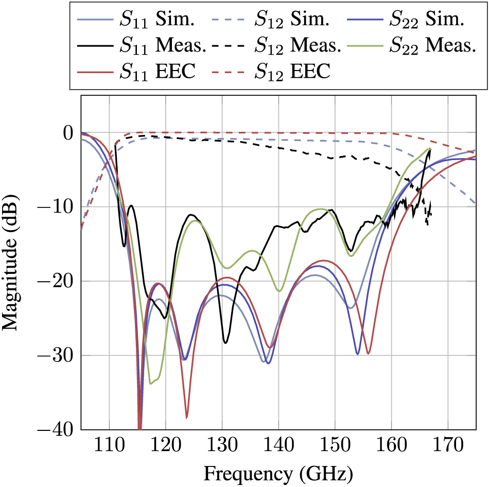
The structure of the proposed transition with  $N$ irises can be approximated by the lossless EEC given in Figure 3. Ports 1 and 2 correspond to the differential microstrip and rectangular waveguide ports defined in Figure 1. A resonator formed by the inductor
  $L_P$ and capacitor
  $C_P$ represents the resonant patch that radiates into the waveguide. This impedance transformation is described by a transformer with ratio
  $1$:
$1$: $N$. By selecting appropriate values for the inductances, capacitances, and line lengths
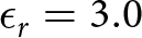
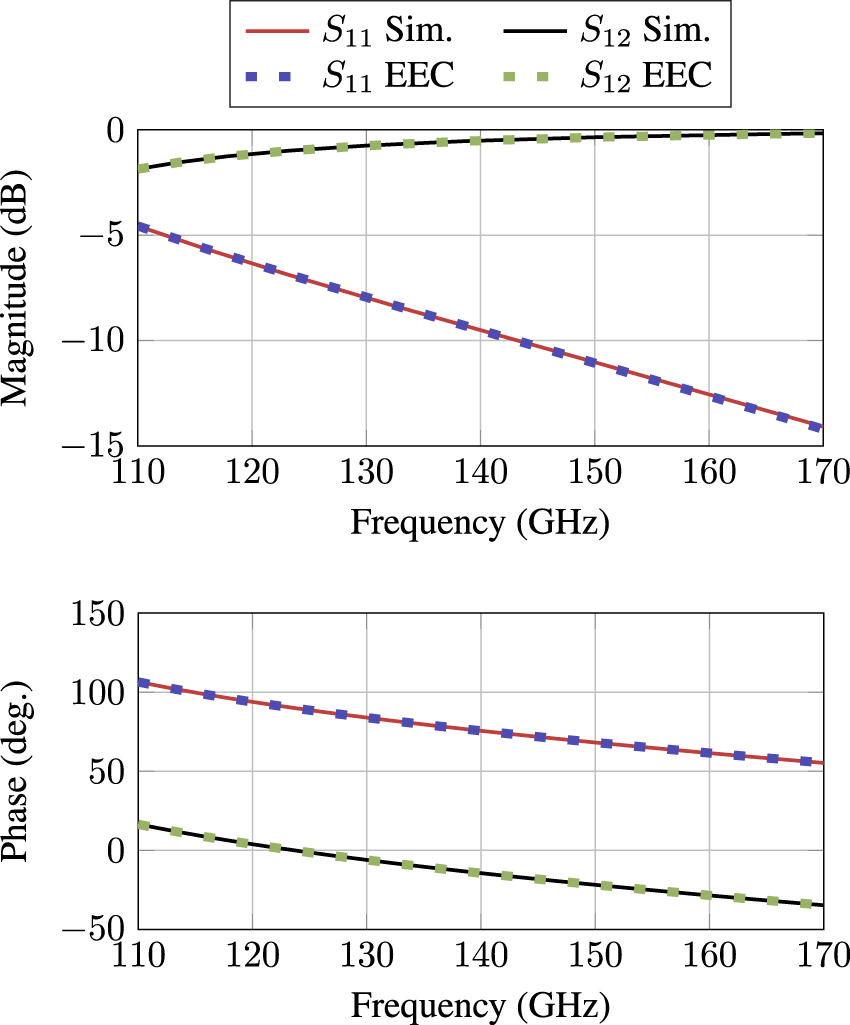
  $l_i$ an impedance matching circuit is achieved that increases the bandwidth of the transition. Figure 2 shows the S-parameters of a full-wave simulated model and the derived equivalent circuit for a transition with three irises (
 $N=3$). The EEC component values are determined through least squares curve fitting based on the results of the full-wave simulation. Table 2 lists their values under the assumption of a reference impedance of
  $100\,\Omega$ at the differential Port 1 and a frequency-dependent reference impedance at Port 2 that mimics the rectangular waveguide characteristics. Although the equivalent circuit is lossless and does not consider higher-order modes, the resulting S-parameters are in good agreement with the full-wave simulation. Figure 2 also shows measured S-parameters for comparison. The measurement procedure is discussed in [Reference Schepers and Krebs1] and therefore not described here.

Figure 2. Simulated and measured S-parameters of the proposed transition and equivalent circuit with three irises.

Figure 3. Generalized lossless equivalent circuit of a waveguide transition utilizing  $N$ irises.
Table 2. Determined component values of the equivalent circuit for  $N=3$
$N=3$

Iris equivalent circuit
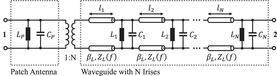
The geometry of each waveguide is fully described by its thickness  $h$ and width
  $w$. The irises are assumed to be symmetrical, so that they always consist of two opposing parts, as illustrated in Figure 4(a). Figure 4(b) shows the chosen equivalent circuit of a single, isolated iris consisting of a shunt inductor and capacitor in conjunction with a dispersive transmission line. This approach allows for an accurate representation of the iris’s significant thickness and enhances the bandwidth of the equivalent circuit [Reference Gatti, Rossi and Dionigi6]. The transmission lines represent the delay introduced by the thickness. In the equivalent circuit of the entire transition in Figure 3, they also account for the distance between the irises. The frequency-dependent line impedance
  $Z_L(f)$ and propagation constant
  $\beta(f)$ are chosen to replicate a WR6.5 rectangular waveguide with
 \begin{equation*}
{\beta}_L(f) = \frac{2 \pi f}{c_0}\sqrt{1-\left(\frac{f_c}{f}\right)^2}
\end{equation*}
\begin{equation*}
{\beta}_L(f) = \frac{2 \pi f}{c_0}\sqrt{1-\left(\frac{f_c}{f}\right)^2}
\end{equation*} \begin{equation}
Z_L(f) = \frac{Z_0}{\sqrt{1-\left(\frac{f_c}{f}\right)^2}}.
\end{equation}
\begin{equation}
Z_L(f) = \frac{Z_0}{\sqrt{1-\left(\frac{f_c}{f}\right)^2}}.
\end{equation}
Figure 4. Single iris inside a rectangular waveguide. (a) Structure and simulation model and (b) EEC.
 $f_c$ represents the cutoff frequency of the
  $\text{TE}_{10}$ mode and
  $Z_0$ denotes the free space wave impedance [Reference Pozar8].
When the reference impedance is equivalent to  $Z_L(f)$, the circuit’s scattering parameters can be expressed as
 \begin{equation}
S_{11} = S_{22} = -e^{-j 2 \beta l} \frac{Y Z_L}{2 + Y Z_L}
\end{equation}
\begin{equation}
S_{11} = S_{22} = -e^{-j 2 \beta l} \frac{Y Z_L}{2 + Y Z_L}
\end{equation} \begin{equation}
S_{12} = S_{21} = e^{-j 2 \beta l} \frac{2}{2 + Y Z_L},
\end{equation}
\begin{equation}
S_{12} = S_{21} = e^{-j 2 \beta l} \frac{2}{2 + Y Z_L},
\end{equation} with  $Y$ being the admittance of the parallel circuit formed by
  $L$ and
  $C$:
$C$:
 \begin{equation}
Y = j 2 \pi f C + (j 2 \pi f L)^{-1}
\end{equation}
\begin{equation}
Y = j 2 \pi f C + (j 2 \pi f L)^{-1}
\end{equation} For a variety of dimensions  $h$ and
  $w$, S-parameters of the iris are simulated using CST and a non-linear least squares fit is applied to determine the component values
  $L$,
$L$,  $C$ and
  $l$ of the equivalent circuit based on Equations (3) and (4). In the simulation, the distance from Ports 1 and 2 to the edge of the iris is deembedded, so that only the thickness of the iris remains. The fundamental
  $\text{TE}_{10}$ mode of the WR6.5 waveguide is excited, so that the E-field vector of the mode is parallel to the iris. Figure 5(a) and (b) shows the resulting relationship between the width
  $w$ and the derived equivalent circuit parameters
  $L$ and
  $C$ for different iris thicknesses
  $h$. With increasing width, the inductance (and therefore its reactance) decreases, causing a more significant influence on the wave propagating through the waveguide. The capacitance increases with iris width; however, since the capacitor’s reactance is proportional to
  $f^{-1}$, it decreases as well. It is likewise evident that a thinner iris exhibits a stronger inductive behavior, while a thicker iris causes a significant increase in its equivalent capacitance. Hence, irises that are oriented as shown in Figure 4(a) are often modeled as a shunt inductor if their thickness is small compared to the dimensions of the waveguide. The resonant frequency
 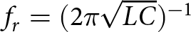 $f_r = (2\pi\sqrt{LC})^{-1}$ of the resonator formed by
  $L$ and
  $C$ as a function of
  $w$ and
  $h$ is given in Figure 5(c). It is large for thin and narrow irises and drops significantly as the width or thickness is increased. In every shown constellation, the resonance frequency is above the frequency range of D-band (
 $110$–
 $170\,\mathrm{GHz}$). Thus, the inductive part of the equivalent circuit predominates, leading to inductive behavior. In general, thin irises tend to give better results for the waveguide transition in terms of bandwidth and matching. In the manufactured transitions, a thickness of
 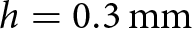 $h=0.3\,\mathrm{mm}$ was chosen for all irises as a compromise between manufacturing feasibility and RF properties.

Figure 5. Iris equivalent circuit component values as a function of iris width  $w$ and thickness
  $h$, derived by least squares fit of full-wave simulated S-parameters. (a) Inductance
  $L$, (b) capacitance
  $C$, and (c) resonant frequency
  $f_r~=~(2\pi\sqrt{LC})^{-1}$.
Exemplary, S-parameters of a full-wave simulated iris and the derived equivalent circuit are given in Figure 6 for dimensions  $h=0.3\,\mathrm{mm}$ and
  $w= 0.2\,\mathrm{mm}$. The plots show excellent agreement over the entire frequency range in both magnitude and phase. In general, the observed fit error is similar for all investigated values of
  $h$ and
  $w$, but tends to rise with increasing iris width and thickness.

Figure 6. S-parameter comparison of full-wave simulated iris and equivalent circuit for  $h~=~0.3\,\mathrm{mm}$ and
  $w~=~0.2\,\mathrm{mm}$.
Impact of manufacturing tolerances
In the frequency range of millimeter waves, manufacturing tolerances often lead to large deviations between simulated and measured characteristics. To some extent, this is also the case for the iris-based waveguide transition as indicated by the discrepancy of the measured S-parameters in Figure 2.
A microscope-based analysis of a set of manufactured transitions with three irises is carried out to estimate the dimensional errors caused by manufacturing tolerances. Figure 7(a) and (b) shows a view into a disassembled split block half. All indicated dimensions are measured using a digital microscope for a total of eight manufactured parts. Similarly, the dimensions of the printed structures marked in Figure 7(c) are evaluated for all manufactured circuit boards. The inspection reveals similar maximum errors of approximately 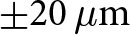 $\pm 20\,\mu\mathrm{m}$ for both the waveguide block and the PCB.

Figure 7. Microscope images of manufactured components. (a) Waveguide split block half, (b) close-up of the marked area showing the irises, and (c) resonant patch surrounded by ground plane and vias.
Based on these results, multiple Monte Carlo simulations are conducted in order to examine the impact of the imperfections on the S-parameters. The simulations involve randomly varying the dimensions of both the printed geometries and the waveguide irises within a range of  $\pm 20\,\mu\mathrm{m}$ relative to their specified dimensions. Additionally, misalignment between the waveguide block and the PCB, as well as variations in the substrate thickness, are considered. A total of 100 simulations are executed, and the resulting S-parameters are depicted in Figure 8(a). Since the variation in the reflection coefficients is comparable for both ports, the curve set for
  $S_{22}$ is not shown for clarity. Although the insertion loss exhibits relative insensitivity to minor geometric variations, significant fluctuations in return loss are noticeable, resulting in a slight reduction in bandwidth. With the exception of single outliers,
  $S_{11}$ remains below
  $-10\,\mathrm{dB}$ throughout the passband, with no notable frequency shift observed. The shaded region in the graph indicates the standard deviation
  $\sigma$ of
  $S_{11}$ around the mean value
  $\mu$ for each frequency point. The measured reflection parameters given in Figure 2 fall within the variation range that results from the Monte Carlo simulation, thereby confirming the anticipated influence of manufacturing tolerances.

Figure 8. Simulated S-parameter deviations caused by manufacturing tolerances. (a) Dimensions of the PCB and the waveguide irises varied, (b) only dimensions of the irises varied, and (c) only dimensions of the PCB varied.
Two additional Monte Carlo simulations are conducted in which the dimensions of either the waveguide irises or the printed planar structures are varied, while all other dimensions remain constant. The resulting S-parameter sets are given in Figure 8(b) and (c). Similar to the previous plot, the standard deviation is highlighted. The results show that the waveguide section exhibits the highest sensitivity to parameter variations at lower frequencies, whereas the variation in  $S_{11}$ for the planar structure is nearly uniform across the passband. Instances where
  $S_{11}$ approaches
  $-10\,\mathrm{dB}$ are more frequently attributed to tolerances in the planar structure. Generally, however, the susceptibility to manufacturing tolerances is similar for the PCB and the waveguide with irises. As the complexity of the transition has been shifted from the PCB to the waveguide, attention must be paid to the manufacturing tolerances in both components.
Finally, the covariances between the variations in S-parameters and changes in geometric parameters are calculated based on the results from the Monte Carlo simulations. The largest covariances and therefore highest sensitivity, is obtained for the parameter  $l_1$ that defines the length of the patch. This is expected, as it directly affects the resonant frequency of the patch. For the waveguide irises, S-parameters are most sensitive to their width
  $w$, i.e. how far they extend into the waveguide.
Investigation of group delay
So far, different designs of iris-based transitions were evaluated in the frequency domain based on their scattering parameters. However, in communication and radar applications, group delay and dispersion play an essential role as well. For a system with phase response  $\varphi(\omega)$, the group delay
  $\tau_g(\omega)$ is defined as
 \begin{equation}
\tau_g(\omega) = -\frac{d\varphi(\omega)}{d\omega} \quad\text{[9]}.
\end{equation}
\begin{equation}
\tau_g(\omega) = -\frac{d\varphi(\omega)}{d\omega} \quad\text{[9]}.
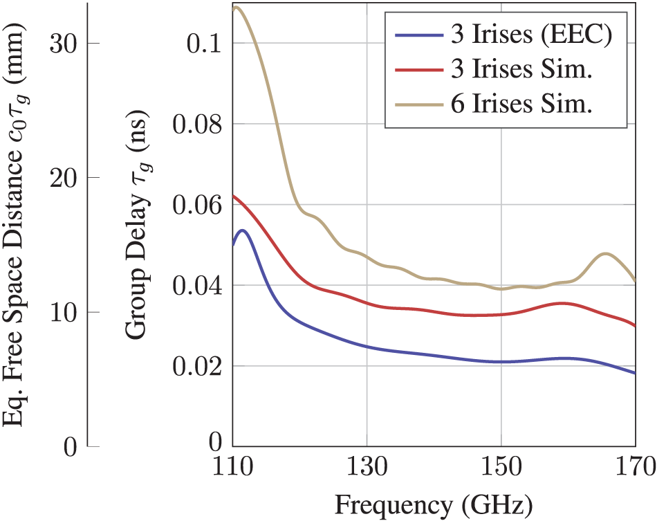
\end{equation}Frequency-dependent variations in the transition’s group delay lead to a distortion of the waveform, resulting in degraded bit error rate or range resolution. Figure 9 shows the group delay of the equivalent circuit and full-wave simulated three-iris and six-iris model determined from their S-parameters using Equation (6). Except for an approximately constant offset, the equivalent circuit and full-wave simulation show a similar trend. In all cases, the group delay is not constant and increases for lower frequencies. This is caused by the dispersive nature of the rectangular waveguide, as well as the irises and the resonant patch. Since the overall length of the waveguide section is larger for the variant with six irises and more resonators are present, its group delay is higher and shows more variation with frequency.

Figure 9. Simulated group delay  $\tau_g$ of the transition designs with three and six irises.
Based on the determined group delay profile, the impact on range profile and resolution in a radar application can be visualized. The secondary vertical axis in Figure 9 represents the equivalent free space distance  $c_0 \tau_g$ a wave is traveling within the corresponding time delay. For the transition with six irises, a variation of up to
  $2\,\mathrm{cm}$ is visible in the specified frequency range. However, the actual influence on radar range resolution is smaller, since the group delay variation is not evenly distributed over the frequency band. In the case of a frequency-modulated continuous wave (FMCW) radar, a point target positioned at a fixed distance
  $r$ results in an intermediate frequency (IF) signal that is a sinusoid with constant frequency, proportional to
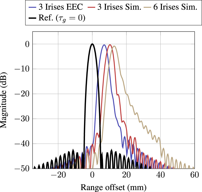
  $r$. The introduction of components with frequency-dependent group delay in the RF path causes the IF frequency to vary proportionally to the variation in group delay. In the range profile, which is obtained by applying a Fourier Transform to the IF signal, this results in a distorted, broadened peak, effectively reducing the radar’s range resolution. Figure 10 shows generated range profiles for all three cases in Figure 9. A monostatic radar with a bandwidth of
  $60\,\mathrm{GHz}$ (
 $110$–
 $170\,\mathrm{GHz}$) is assumed and a Hamming window is used prior to the Fourier Transform.

Figure 10. Influence of simulated group delay from Figure 9 on range profile peak shape and shift in a radar application.
In comparison to the black reference curve (Ref.) representing 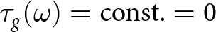 $\tau_g(\omega) = \text{const.} = 0$, it is evident that the peaks are shifted and distorted. The shift is caused by the constant component of the group delay. Since the variation of the group delay is a non-linear function of frequency, the energy of the IF signal is not uniformly distributed, leading to an asymmetric shape of the peak. For the transition utilizing three irises, the effect is negligible, while for the variant with six irises, it becomes clearer. The influence on the
  $3\,\mathrm{dB}$ peak width is generally small; however, the
  $20\,\mathrm{dB}$ width is increased significantly. In scenarios where weak targets are close to strong targets, masking effects may occur.
If the group delay characteristics of a system are known, it is possible to compensate them in post-processing. An example is given in [Reference Wittemeier, Sievert, Dedic, Erni, Rennings and Pohl10]. Especially when the transition is followed by a long rectangular waveguide section, the influence of dispersion is dominant and should be compensated to maintain the resolution of the system.
Application in radar frontends
As described in Section I, iris-based waveguide transitions represent an alternative to other broadband transitions due to their compact size and the elimination of additional process steps during PCB manufacturing. As example of a practical application, a variant with six irises and adapted center frequency of  $120\,\mathrm{GHz}$ is utilized in the realization of a multichannel, broadband radar frontend. Since the radar features two dedicated receive and transmit channels, a total of four transitions are required. Figure 11(a) shows a section of the frontend’s circuit board, including the four patches surrounded by guiding holes for the waveguide block and the frontend MMIC. As in the initial transition design,
  $0.127\,\mathrm{mm}$ thick Rogers RO3003 is used as the substrate. The differential microstrip lines that feed the outer transitions run in a 90-degree bend, causing a length difference between the inner and outer traces. By adding spline-shaped length-matching sections to the inner trace, the total lengths are kept equal to maintain the differential mode. In addition to the RF components and waveguide transitions, the frontend PCB also includes power supply generation, a PLL for chirp generation, as well as IF filters and amplifiers. The total size of the PCB is
  $10\,\mathrm{cm}$ by
  $7\,\mathrm{cm}$. The waveguide block that rests on the PCB and contains the irises is shown in Figure 11(b). It features a custom flange on the back side that allows to mount different antenna types. In this example, a 3D-printed aluminum waveguide block that incorporates rectangular horn antennas with a directivity of
  $17\,\mathrm{dB}$i is used, as recognizable in Figure 12(a). Four additional rectangular horn antennas with smaller apertures can be seen, which are utilized for a secondary frequency band located around
  $240\,\mathrm{GHz}$, allowing dual-band operation. In this case, direct transitions from the frontend MMIC to rectangular waveguides are utilized, which are not addressed in this paper.

Figure 11.  $120\,\mathrm{GHz}$ radar frontend utilizing four iris-based transitions. (a) PCB close-up showing the four transitions, differential microstrip lines and frontend MMIC, and (b) waveguide block with irises, which is placed onto the PCB.

Figure 12. Radar measurement. (a) Setup with radar frontend (left) and two cylinders as targets (right) and (b) range profile with and without targets after group delay compensation.
Figure 12(a) shows the radar frontend in operation. Two closely spaced metal cylinders with a  $2.5\,\mathrm{cm}$ diameter placed at a distance of approximately
  $35\,\mathrm{cm}$ serve as targets. For the measurements, the FMCW chirp duration is set to
  $100\,\mu\mathrm{s}$ across a bandwidth of
  $40\,\mathrm{GHz}$ (
 $100$–
 $140\,\mathrm{GHz}$). The down-converted IF signals are digitized using a Rohde & Schwarz RTO2064 oscilloscope at a
  $50\,\mathrm{MHz}$ sampling rate and an effective vertical resolution of 16 bits. Figure 12(b) shows range profiles determined by applying an FFT to the recorded IF signals. As an additional post-processing step, the influence of frequency-dependent group delay has been compensated to prevent distortion of the peaks, as discussed in the fourth section. It should be noted that other, approximately constant delays caused by microstrip lines and the frontend MMIC itself are not compensated in this example, resulting in an arbitrary definition of the range axis’ zero point. Depending on the intended application, a suitable absolute zero point may be chosen and the range axis shifted accordingly.
The depicted curves represent range profiles measured with and without the two cylinders placed. Four of the most prominent peaks are marked. The first peak, which is located at a negative range due to the group delay compensation, is caused by crosstalk between transmit and receive channels in the frontend. Peak 2 also results from crosstalk, in this case, however, between the receive and transmit antenna apertures. Peaks 3 and 4 represent the two cylinders separated by  $2.1\,\mathrm{cm}$. They are therefore not recognizable in the reference measurement. The peaks exhibit a
  $3\,\mathrm{dB}$ width of
 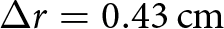 ${\Delta r=0.43\,\mathrm{cm}}$ which is close to the ideal value of
  ${\Delta r=0.37\,\mathrm{cm}}$ given a bandwidth of
  ${B=40\,\mathrm{GHz}}$ resulting from basic signal and radar theory
 \begin{equation}
\Delta r = \frac{c_0}{2B} \quad\text{[11]}.
\end{equation}
\begin{equation}
\Delta r = \frac{c_0}{2B} \quad\text{[11]}.
\end{equation}Since the RF output power of the frontend is not constant, but varies over frequency, this difference is expected. The influence may be reduced by applying an equalization prior to the FFT. Nevertheless, this example shows that the developed transition is suitable for a broadband multichannel radar application. The simple planar structure allows for relatively straightforward PCB manufacturing without the need for a backshort or complex depth milling operations on the circuit board.
Design guidelines
Based on the derived equivalent circuit and gained experience during the design of iris-based transitions, general guidelines were defined that lead to a good starting point for an optimization:
• The PCB substrate permittivity must be sufficiently high to allow the realization of a resonant patch that is smaller than the waveguide’s footprint. Choosing
 $\epsilon_r = 3.0$ is usually sufficient. Much higher permittivity values will result in a reduced bandwidth.
• The resonant patch surrounded by a ground plane and shielding vias should be designed first. Optimize the resonant frequency to the intended center frequency of the transition.
• Initially, the waveguide should not contain more than three irises. Additional irises may be added later if the achieved bandwidth is not sufficient. No further improvement in bandwidth is expected beyond six irises.
• A quarter guided wavelength at the intended center frequency is a good starting point for the distance between the irises.
• The irises should be as thin as possible (i.e., a low value of
$h$), while respecting manufacturing limitations.• Too small distance between the first iris and substrate can lead to undesired radiation through the cutout in the waveguide that is required to feed the patch.

Conclusion
In this paper, the properties of novel D-band waveguide transitions that comprise a resonant patch on the PCB and multiple irises within the waveguide are studied. The irises form an impedance matching network that is modeled using lumped elements. The influence of iris width and thickness and the impact of manufacturing tolerances are investigated by parametric analysis and Monte Carlo simulations. Further, the group delay characteristics are determined and the resulting distortion is demonstrated. As an application example, transition designs with six irises are utilized in a compact multichannel radar frontend with  $40\,\mathrm{GHz}$ bandwidth and measured range profiles are presented. Using the derived design guidelines, a straightforward customization of iris-based transitions for different applications and frequency bands is possible.
Competing interests
The authors declare none.

M. Schepers received his M.Sc. in electrical engineering from RWTH Aachen University, Germany, in 2022. He is a research associate at Fraunhofer FHR in the Antenna Technologies and Material Measurement team of the Frontend & Systems department. His research interests include the design of antennas and passive components for millimeter-wave radar systems.

C. Krebs is a lecturer at Koblenz Technical University, Germany, for printed circuit board (PCB) design and PCB high-speed applications and is head of the department Frontend & Systems. His activity at Fraunhofer FHR is the development of new concepts for high-frequency systems in industrial applications of the Integrated Circuits and Sensor Systems department.


 Open access