Introduction
Recent technological advancements in communication systems at microwave, millimeter, and optical frequencies demand the design and development of multifarious devices. Frequency selective surfaces (FSSs) have evolved as one of the most researched fields to meet the standards of modern and advanced communication systems. FSS-based absorbers have a wide variety of applications in stealth technology [Reference Priyanka, Alegaonkar and Baskey1], electromagnetic (EM) shielding [Reference Shukoor and Dey2], radar cross section reduction [Reference Das and Mandal3], EM energy harvesting [Reference Amin, Almoneef, Siddiqui, Aldhaeebi and Mouine4], and so forth. Most of the reported FSS-based absorbers are designed on rigid, inflexible, and hard substrate materials, whereas real-world applications like military aircrafts [Reference Zhang, Dong, Mou, Chen, Rihong and Zhang5], fighter jets [Reference Hannan, Tariqul Islam, Soliman, Sahar, Singh, Faruque and Alzamil6], torpedoes [Reference Chejarla, Thummaluru and Chaudhary7], radars [Reference Kang, Zeng, Duan, Jing, Hao, Song, Wang and Zhang8], missiles [Reference Zhou, Qin, Liang, Meng, Xu, Smith and Liu9], wearable functional devices [Reference Gong, Hao, Li, Li and Xiong10], RF sensors, bio-interfaces [Reference Wang, Zhao, Wang, Luo, Xie, Zhan, Kim, Wang, Liu and Ying11], shielding human and vehicles from battlefield radars [Reference Gaganpreet, Sheokand, Chaudhary, Srivastava, Ramkumar and Ramakrishna12], etc. involve curved or nonplanar surfaces. Therefore, developing a flexible, polarization-independent, lightweight, and cost-effective absorber for applications, which demand curvilinear surfaces and conformal designs, is the need of time.
Various types of flexible substrates have been utilized by the researchers to realize the conformal behavior of the absorbers, like PET (Polyethylene terephthalate) [Reference Kalraiya, Kumar Chaudhary and Kumar Gangwar13, Reference Kalraiya, Chaudhary, Abdalla and Gangwar14], Silicon rubber [Reference Weiwei, Jin, Zeng, Zhang, Zhang and Zhang15], PDMS (Polydimethylsiloxane) [Reference Jeong and Lim16], PVC (Polyvinyl chloride) [Reference Aqilafif, TeguhYudistira and Qalbina17], textile [Reference Gaganpreet, Sheokand, Chaudhary, Srivastava, Ramkumar and Ramakrishna12, Reference Lee, Ki Kim and Lim18], polymide [Reference Deng, Kun, Sun, Yang, Yin, Li, Chi and Li19] and paper [Reference Tirkey and Gupta20]. Few absorber geometries have been constructed by using ultrathin substrates, like Taconic [Reference Zargar, Rajput, Saurav and Koul21], RT Duroid 5880 [Reference Joy, Baghel, Tabassum Nazeer and Singh22, Reference Luo, Weiliang, Yufeng, Jin, Fan and Zhu23], and FR4 [Reference Chejarla, Thummaluru and Chaudhary7, Reference Chaitanya, Peshwe, Ghosh and Kothari24, Reference Kalraiya, Ameen, Kumar Chaudhary and Kumar Gangwar25] where the structures can be bent upto certain angles due to their low profiles. While they offer effective flexural strength, they are not ideal for applications involving prolonged and repetitive bending. Similarly, multi-layered geometries have been reported [Reference Xia, Wei, Liu, Zhang, Guo, Chengli, Bie and Jiang26, Reference Hang, Wei, Lin, Liu, Miao, Bie and Jiang27]. Graphene and other composites have also been attempted to design flexible absorbers in [Reference Anjali, Rengaswamy, Ukey, Stephen, Krishnamurthy and Subramanian28]. However, it is very difficult to achieve flexibility while maintaining absorptivity in those types of design configurations. Further, their fabrication procedures are complex and expensive. In [Reference Xin, Binzhen, Wanjun, Junlin and Junping29] absorber fabricated on a polyimide material using a complex laser ablation technique is presented. Additionally, a dual-layer triple-band flexible absorber was proposed on neoprene rubber, incorporating copper foil tape as a conductor [Reference Kaur, Upadhyaya, Palandoken and Gocen30]. However, due to the manual fabrication process, scaling up for large-scale applications presents significant challenges.
In this paper, a 3D-printed low-cost, lightweight, and conformal FSS-based absorber is designed and developed. Two concentric square loops are fabricated at different heights utilizing the 3D printing technology to realize the dual-band absorption at two different frequency bands (S and C-bands). Owing to the use of the perforated topology, the geometry is flexible and can be bent to different curvatures, thereby satisfying the conformal behavior. The square loops have also been made at different heights, thus adding another degree of freedom to the design, unlike the fixed-height planar structures. The absorption mechanism is explained with the help of impedance curves and surface current distributions. The prototype of the presented absorber has also been built and its absorptivity responses are measured for leveled and bent surfaces, which concur with the simulated results.
Design and analysis
Unit cell response
Figure 1 illustrates the unit cell configuration consisting of two concentric square loops with different heights resonating at two different frequencies. The square loops are elevated on a base layer with 0.3 mm thickness (H1). The concentric square loops have heights of 1 mm (H2) and 1.5 mm (H3) for the outer loop and inner loop, respectively. The 3D printer-compatible filament PLA (polylactic acid) substrate is used as the constituent dielectric (marked by grey color) with a dielectric constant of 2.1 and a loss tangent of 0.07. The metal ground plane at the back side of the structure and the conducting surfaces on the top of the square loops are considered copper metal with thicknesses of 0.065 mm each. The master-slave boundary conditions in the x-y axes and Floquet port excitation in the z-axis have been applied around the unit cell to analyze the structure for an infinite unit cell arrangement.

Figure 1. Proposed unit cell design P = 20 mm, S1 = 19 mm, S2 = 15 mm, S3 = 14 mm, S4 = 10 mm, T1 = 2 mm, T2 = 2 mm, G1 = 0.5 mm, G2 = 0.5 mm, H1 = 0.3 mm, H2 = 1 mm, H3 = 1.5 mm.
Figure 2 shows the reflectivity and absorptivity responses of the presented structure. The design exhibits a dual-band response having resonances at 3.32 GHz (S-band) and 5.46 GHz (C-band) with reflectivities of −20 dB and −15 dB, respectively, which correspond to absorptivities of 99% and 97%, respectively. This indicates that only 1% and 3% of incident EM wave are accounted as reflection loss at first and second frequencies, respectively. The corresponding full widths at half maximum bandwidths are observed as 230 MHz (3.21–3.44 GHz) and 450 MHz (5.27–5.72 GHz). The individual impacts of each loop have been studied in Fig. 3. It is clearly observed that the inner loop (design-I) contributes toward the second band resonating at 5.46 GHz and the outer loop (design-II) contributes toward the first band resonating at 3.32 GHz.

Figure 2. Absorptivity and reflectivity curves of the proposed dual-band absorber.

Figure 3. Effect of individual square loop designs on absorptivity curves.
Equivalent circuit model
The equivalent circuit model of the presented structure is illustrated in Fig. 4. L1 and L2 are the effective inductances corresponding to the lengths of the outer and inner square loops, respectively. R1 and R2 are resistances due to the finite conductivity of the top copper metal of the loops and represent small ohmic losses. C1 represents the equivalent capacitive between the adjacent unit cells; whereas C2 shows the capacitance between the inner and outer loops of the unit cell. The dielectric substrate is represented by a transmission line, and the bottom metal plane can be considered a short circuit. This shorted circuit transmission line is represented by an equivalent inductance Z d. Thus, the total impedance (Z total) of the presented structure can be calculated as

Figure 4. Equivalent circuit model of the proposed absorber: (a) contribution of individual segments, (b) overall circuit model, and (c) comparison of equivalent circuit model response and simulated result of the absorber.
where Z i is the equivalent impedance of the inner loop (a combination of R2, L2, and C2) and Z o is the equivalent impedance of the outer loop (a combination of R1, L1, and C1). By regulating different geometric dimensions of each of the square loops as well as the substrate properties, their corresponding impedances can be controlled, and resonances can be generated accordingly.
The Advanced Design System software is used to determine the values of the circuit parameters of the equivalent circuit model. After optimization, the determined values are as follows: R1 = 7.68 Ω, L1 = 1.01 nH, C1 = 0.78 pF, R2 = 1.96 Ω, L2 = 1.98 nH, and C2 = 0.2 pF. The comparison curves, showing the reflectivity responses evaluated from the calculated results of the equivalent circuit model and those from the simulation software High Frequency Structure Simulator (HFSS) Version 14.0, are depicted in Fig. 4(c). It is clearly evident that both curves exhibit significant alignment, thereby validating the correctness of the proposed equivalent circuit model.
Parametric analysis
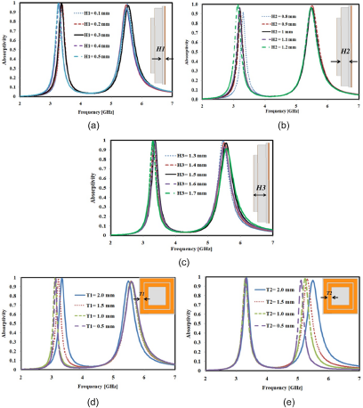
The effects of variation in different design parameters are studied and illustrated in Fig. 5(a–e). Figure 5(a) depicts the variation of the base substrate height H1, which shows that both absorption peaks are shifted marginally. This base substrate is used for the support during fabrication, and hence is kept as minimal as possible (= 0.3 mm). Owing to the advantage of 3D printing technology, the heights of each of the square loops can be realized with different values, and therefore, their variations are analyzed individually. Figure 5(b) represents that with the increase in the height of the outer square loop (H2), a slight shift in the resonance frequency is observed in the lower band, whereas the higher band remains constant.

Figure 5. Study of variation in design parameters on the absorptivity responses: (a) H1, (b) H2, (c) H3, (d) T1, and (e) T2.
While varying the height of the inner square loop (H3), the change in the absorption frequency of the higher band is more prominent than that of the lower band, as observed in Fig. 5(c). Figure 5(d) and (e) represent the variation in the width of the outer loop (T1) and inner loop (T2), respectively. It is observed that the corresponding resonance frequencies shift toward the lower side with the decrease in the widths. The inductances are increased with smaller values of metallic widths that cause the redshift of the absorption bands.
Impedance graph
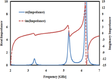
One of the important parameters that should be investigated in absorber geometry is its input impedance. Since the proposed structure is terminated with a metal ground, there is no transmission (S 21 = 0), and the absorptivity can be determined from the reflection coefficient (S 11) only. A near-unity absorption response can be obtained, if the input impedance (Z in) of the geometry can be matched with the free space impedance (377 Ω). The real and imaginary parts of the input impedance of the proposed absorber are illustrated in Fig. 6, which is determined using Equation 2. The values of real and imaginary impedances obtained at resonant frequencies are tabulated in Table 1. It is observed that the maximum absorption is perceived at the resonant frequencies as the real part of Z in is close to unity and its imaginary part is close to zero.
 \begin{equation}{Z_{in}} = \,\sqrt {\frac{{{{\left( {1 + \,{S_{11}}} \right)}^2} - {{\left( {{S_{21}}} \right)}^2}}}{{{{\left( {1 - \,{S_{11}}} \right)}^2} - \,{{\left( {{S_{21}}} \right)}^2}}}} \end{equation}
Figure 6. Real and imaginary impedance curves.
Table 1. Values of real and imaginary impedances for the frequencies of resonances

Surface current and electric field distribution
The absorption mechanism has further been examined by analyzing the surface current and electric field distributions of the proposed design at two resonant frequencies (3.32 GHz and 5.46 GHz), as illustrated in Fig. 7. The concentration of surface current is observed at the inner loop at 5.46 GHz and the outer loop at 3.32 GHz with anti-parallel orientation on the top and bottom layers of the structure, thus producing the magnetic field excitation formed due to the accumulation of circulating current. The electric field excitations are mostly observed in the metallic patches. At resonance frequencies, both magnetic and electric fields excite at the same time and achieve the maximum absorptivity.

Figure 7. Surface current distribution at (a) top surface, (b) bottom surface, and (c) electric field distribution at two different absorption peaks.
Polarization and oblique incidence angle variation
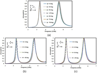
The absorption responses under different polarization angles (ϕ) of the proposed design is depicted in Fig. 8(a). This study is carried out for a constant incident EM wave vector direction, while varying both magnetic and electric fields with an angle ranging from ϕ = 0 degree to 90 degree with a step size of 15 degree. A similar absorption behavior is observed for all the cases, thus confirming the structure as polarization-independent. The impacts of the incident angle variation on the absorption characteristic under the transverse electric (TE) and transverse magnetic (TM) polarization cases are investigated in Fig. 8(b) and (c), respectively. With a steady direction of the electric field, while varying the incident angle (θ) of the magnetic field and direction of wave propagation, the TE mode is analyzed. Alternatively, with a steady direction of the magnetic field, while varying the incident angle (θ) of the electric field and direction of wave propagation, the TM mode is analyzed. For both cases, the absorption magnitudes have been observed to remain almost constant up to 45 degree incident angle, but a decrease in the absorption magnitude is observed with a further increase in the angle of incidence. As a result, it has been concluded that stable absorption responses are maintained up to a 45-degree angle for both TE and TM modes in both absorption bands.

Figure 8. Simulated absorptivity patterns (a) at different angles of polarization (ϕ), and at varied angles of incidence (θ) under (b) TE polarization, and (c) TM polarization.
Conformal analysis
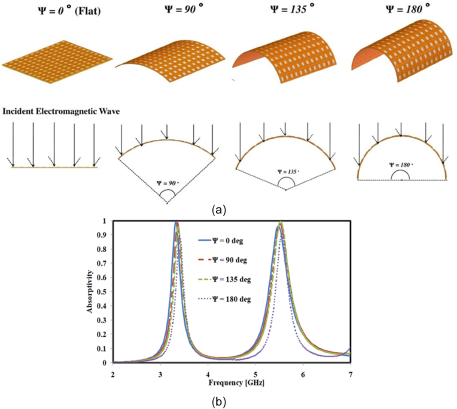
The conformal behavior of the proposed design is investigated by bending the structure on various 3D printed cylindrical mockup models having angles of curvature at 180 degree, 135 degree, 90 degree, and 0 degree, as depicted in Fig. 9(a). With the increase in the arc angle, the radius of curvature (ROC) decreases; thus, the flat surface has the radius maximum (infinity) and the 180 degree curvature has the radius minimum. The absorption behavior of the proposed design is simulated for different arc angles and it is observed in Fig. 9(b) that the response remains relatively stable with a slight frequency shift with the decrease in the angle. It is worth noting that owing to the use of 3D printing technology, the proposed geometry can be wrapped on different cylindrical surfaces even though the total height of the structure is 1.8 mm (H1 + H3 = 0.3 mm + 1.5 mm),which is a comparatively larger thickness to be bent.

Figure 9. (a) EM wave incidence on different ROC on which the absorber structure is wrapped, (b) simulated absorptivity responses for different ROC values.
Fabrication and measurement results
Figure 10(a) shows the proposed absorber design fabricated using 3D printing technology with a 12 × 12 unit cell arrangement having a total size of 240 × 240 mm2. Commercially available PLA filament is used for the fabrication of the substrate pattern using the Pratham 6.0 3D printer by Make3D.in. Different heights have been realized for different square loops on the top of the base substrate using a single-step fabrication. Afterward, the back side ground and top conducting surface are realized using 0.065 mm thick adhesive copper tape. The patterns have been cut from the copper tape using a Skycut C24 vinyl cutter and pasted on the 3D printed substrate accurately.

Figure 10. (a) Fabricated prototype of 3D printed dual-band absorber. (b) Simulated and measured responses of the presented absorber.
The conventional free space method has been employed for the measurement comprising an assembly of two horn antennas connected to a handheld Anritsu vector network analyzer. The prototype has been mounted in the middle of an absorbing wall, where the antennas are placed on the same side of the structure in close proximity. The reflection response is first measured for a copper plate of identical dimensions and then it is replaced with the original prototype. The difference in reflection between the original prototype and that of the copper plate gives the real reflection coefficient (or absorption). Figure 10(b) shows the comparative analysis of the simulated and measured absorption responses, and they concur well with each other except for minor undulation due to size limitation and fabrication imprecision. The bending analysis has also been studied by wrapping the structure on mock-up cylindrical models having different arc angles as shown in Fig. 11(a). Stable absorption responses are observed for different radii of curvature, as illustrated in Fig. 11(b).

Figure 11. (a) Measurement setup of the fabricated prototype wrapped on mockup models having different radii of curvature. (b) Measured absorptivity responses corresponding to different models.
A comparison of the absorber presented in this study with flexible absorbers from prior research is outlined in Table 2. The analysis reveals that despite its relatively large thickness, the presented absorber maintains conformality due to its perforated topology. Additionally, the absorber’s resonators are constructed at varying heights, providing an additional level of design flexibility not found in fixed-height planar structures having resonators on same level.
Table 2. Comparative study of the proposed absorber with respect to existing literature on flexible microwave absorbers

λ: Wavelength (= 90.36 mm) to lowest resonance frequency (3.32 GHz); NR = not reported.
Conclusion
A 3D-printed polarization-insensitive low-cost lightweight and flexible FSS-based dual-band absorber is presented. Two concentric square loops with different substrate heights are designed for exhibiting dual-band responses at 3.32 GHz and 5.46 GHz resonating in S and C bands, respectively, with more than 97% absorptivities. The absorption behavior has been explained with the help of impedance graphs and surface current distributions. The prototype has also been fabricated and its absorptivity responses are measured for leveled and bent surfaces at different radii of curvature which concur with the simulated results, thereby confirming its flexible behavior.
Acknowledgements
The authors acknowledge the support of Applied Electromagnetic Laboratory of IIT Indore for providing testing and measurement facilities and AICTE IDEA Lab, Acropolis, Indore for fabrication resources.
Funding
This research received no external funding.
Competing interests
The authors declare that they have no known competing financial interests or personal relationships that could have appeared to influence the work reported in this paper.

Gaurav Chaitanya earned his Bachelor’s degree in Electronics & Communication Engineering in 2007 followed by a Master’s degree from IES, IPS Academy, Indore (affiliated to RGPV, Bhopal, India) in 2012. He boasts over 17 years of teaching experience at the Acropolis Institute of Technology and Research, Indore, India. Currently, he pursues his doctoral research at the Indian Institute of Information Technology, Nagpur, India. He holds Senior Membership at IEEE and Life Membership at ISTE. His research interests encompass Frequency Selective Surfaces (FSS), Metamaterials, and Absorber design.

Dr. Paritosh Peshwe completed his Master’s degree in Microelectronics from BITS, Pilani in 2013, and attained his PhD in Antenna Design from VNIT, Nagpur in 2019. His expertise lies in Antenna Design and Wireless Communication. Currently, he serves as an Assistant Professor in the Department of Electronics and Communication Engineering at the Indian Institute of Information Technology, Nagpur, and is a member of IEEE.

Dr. Saptarshi Ghosh holds an MTech and PhD in Electrical Engineering from the Indian Institute of Technology, Kanpur, India, awarded in 2013 and 2017 respectively. He subsequently worked as a Postdoctoral Research Fellow at Chung-Ang University, Seoul, Korea, before joining the Indian Institute of Technology Indore, Madhya Pradesh, India, where he presently serves as an Associate Professor. His research expertise spans electromagnetics, frequency selective surfaces, reconfigurable circuits, and metasurfaces. Dr. Ghosh actively contributes as a referee for various IEEE Journals and Conferences, and he holds membership in IEEE and serves as an Associate Editor of IEEE Antennas and Wireless Propagation Letters.

Dr. Ashwin Kothari obtained his PhD from Visveswariya National Institute of Technology, Nagpur in 2010. His research interests include Communication, Signal processing, Rough Sets, Cognitive Radio, Antennas, and Embedded systems. Currently, he holds the position of Professor and Head in the Department of Electronics and Communication Engineering at VNIT, Nagpur. Additionally, he has served as an In Charge Dean at the Indian Institute of Information Technology, Nagpur.


