Introduction
The continuous need for high data rate (DR) and more mobile applications has been a major driver in rapid adoption of 5G and WiFi7, as well the intense research activity for 6G [Reference Balteanu, Thoomu, Pingale, Venimadhavan, Sarkar, Choi, Modi, Drogi, lee and Agarwal1–Reference Chen, Gaal, Montojo and Zisimopoulos3]. According to the International Telecommunication Union (ITU), there were more than 8.58 billion mobile subscriptions in use worldwide in 2022, compared to a global population of 7.95 billion (Fig. 1). 5G smartphones uses sub-6 GHz bands and mmWave spectrum [Reference Pehlke, Brunel, Walsh and Kovacic4] together with other RF technologies such as ultra-wideband (UWB), sensing, and computation techniques [Reference Giordano, Polese, Roy, Castor and Zorzi5, Reference Dotlic, Connell, Ma, Clancy and McLaughlin6]. 5G will continue to grow fueled by capability to support a variety of new and enhanced services, for example vehicle-to-vehicle (V2X) communications, factory automation, eHealth [Reference Gharba, Xiao, Cao, Eichinger, Hecker, Kranzfelder and Ostler7], autonomous vehicle [Reference Barbi, Antón, Mrozowski, Inca and Monserrat8], and Internet of things [Reference Al-Fuqaha, Guizani, Mohammadi, Aledhari and Ayyash9]. Today, mobile phones are ubiquitous and for the 650 million smartphones sold worldwide in 2022 more than half are 5G capable. 5G smartphones need to carry over the legacy voice (2G/3G) and need to integrate sub-6 GHz bands known as frequency range 1 (FR1). There is a significant pressure to maintain a balance between the increase functionality and the added cost and size associated with it. As a result, a limited number of 5G stock-keeping units include mmWave modules. There are many advanced developments related to 5G bands, as well the adoption of 6G. It is anticipated that upcoming 5G+ smartphones will incorporate new sensing and interface circuitry to accommodate the new RF bands (Fig. 2) associated with this next generation.

Figure 1. Smartphone subscription and worldwide population (ITU).

Figure 2. 5G/6G frequency bands.
The main goals for 5G new radio are to achieve low latency and DRs of 1 GB. To achieve these DRs, 5G smartphones use 4 × 4 multiple input multiple output (MIMO) and carrier aggregation (CA) [Reference Balteanu, Drogi, Choi, Lee, Modi, Khesbak and Agarwal10]. For a wireless system with k MIMO channels, the capacity is determined by the Shannon’s formula as:
 \begin{equation}\,\,\,\,\,\,\,\,\,\,\,\,\,\,\,\,\,\,\,\,\,\,\,\,\,\,\,\,\,\,\,\,\,\,\,\,\,\,\,\,\,\,\,\,\,\,\,\,\,\,\,C = {B_w}\sum\limits_{k = 1}^k {{{\log }_2}(1 + \frac{{{e_k}{S_k}}}{{{N_x} + {I_k}}}} )\end{equation}
where Bw is channel bandwidth, Sk is the transmit power for the multiplexed level k through MIMO, Ik is in-band interference, ek is the increase through use of envelope tracking (ET) or average power tracking (APT), and Nx is in band thermal noise. With the introduction of mmWave bands, as well the proposal to introduce new bands for 5G/6G [11], the frequency bands are divided into several frequency ranges (Fig. 2):
• FR1 includes all existing 4G bands and new 5G bands and corresponds to 410 MHz–6 GHz; sub-6 GHz bands. These bands are the backbone of 5G deployment and carry the bulk of data traffic right now.
• Frequency range 2 (FR2) includes new mmWave bands 24.25–71 GHz. Just several smartphones carry mmWave module due to size, power consumption, higher RF propagation loss, and extra cost.
• Frequency range 3 includes bands from 10 to 20 GHz and there are initial discussions in 3rd Generation Partnership Project (3GPP)for future deployment/use for 5G.
• Frequency range 4 covers 52.6–71 GHz and is expected to be used in autonomous vehicles and vehicular radars.
• Frequency range 5 covers 95–325 GHz and will be part of 6G deployment.
Low latency is the prerequisite for real-time applications, such as self-driving and autonomous cars, as well smart machines communicating in real time. Reliable high DR and low latency are important in connecting smart devices in 5G. A typical 5G RF front-end (RFFE) module for 5G mobile devices has six to nine antennas for under 6 GHz space (5G, WiFi, Bluetooth, GPS, and UWB) and 8/16 channels FR2 mmWave module (Fig. 3). Actual smartphones are equipped with multiple antennas that can cover various frequency bands. These antennas are strategically chosen based on the most optimal propagation path to communicate with the base station. To ensure coverage across multiple bands, aperture tuners (ATs) and impedance tuners (ITs) are used to adjust for any mismatch. The selection of the best propagation path is determined by evaluating the maximum signal-to-noise plus interference ratio (SINR).

Figure 3. 5G smartphone RF front-end modules architecture.
Cellular RFFE modules and power amplifiers
With the 5G band proliferation there are several RFFE modules in a mobile device covering more than 50 bands. The power amplifier (PA) for RFFE is integrated in the same module (Fig. 4) with several acoustic filters, silicon on insulator (SOI) RF switches, low noise amplifiers (LNAs) for time division duplex (TDD) case, ET circuits, and serial parallel mobile industry processor interface (MIPI RFFE) circuitry [Reference Balteanu12]. Sub-3 GHz bands provide primary long-term evolution (LTE)cellular coverage and the new 5G bands provide the primary increased capacity using MIMO technology and CA.
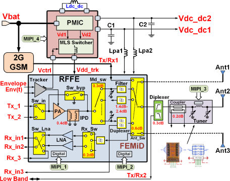
Figure 4. 4G/5G RF front-end module structure.
One of the most important parts in the RFFE is the PA. With the adoption of 256QAM for 5G uplink (UL)the PA linearity, expressed through error vector magnitude (EVM), is challenging to be achieved (less than 1.85%), although 5G allows 4–5 dB maximum power reduction. Few techniques have been used to meet the efficiency and linearity requirements, the most extensively used and researched being Doherty and ET PAs [Reference Doherty13–Reference Grebennikov15]. The adoption of both techniques has been made feasible through advancements in digital signal processing and technology scaling, such as 3 nm/5 nm FinFET. Although Doherty techniques are known for their high efficiency, they do have limitations in terms of broadband operation, back-off mode operation, and handling load mismatch [Reference Zenteno, Isaksson and Händel16–Reference Singh, Mul, Nemati, Alavi MS and Vreede18].
Doherty amplifiers, with n-away structures to increase the bandwidth (BW) (Fig. 5), are currently used in 5G base station [Reference Wong, Watanabe and Grebennikov19]. Doherty amplifiers require digital predistortion (DPD) that presents some challenges, especially for higher modulation BW in 5G and future 5G+ and 6G. Current 5G systems use DPD but this technique present several challenges:
• With the increase channel BW, e.g., 100 MHz LTE for FR1, the DPD instantaneous BW is 3–5× higher and can be as high as 400–500 MHz. Higher DPD BW is required to reduce the PA memory effects and this requires also high BW for the observation path. Assuming 1 GHz modulation BW for FR2 this task is even more difficult [Reference Li, Pang, Zhang, Yamazaki, Wang, Luo, Chen, Liao, Tang, Wang, Fu, You, Oshima, Hori, Park, Kunihiro, Shirane and Okada20–Reference Wang, Asbeck and Fager22].
• To get higher DR 5G smartphones use multiband and CA and therefore there is the need for separate DPD processing paths.
• The new 5G FR1/FR2 bands use TDD [Reference Pehlke23] and one of the main challenges comes from the PA operating on/off in a duty cycle and going through different thermal profiles. DPD must adapt in real time to thermal effects, which may be very challenging for mobile devices.
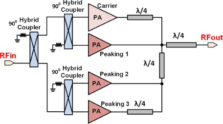
Figure 5. Three-way Doherty PA.
Actual PAs in mobile devices are broadband class E PAs and are operated most of the time with an ET controller. ET technique was first introduced by Kahn in paper [Reference Kahn14] and worked for low signal modulation BW. With the fast development of digital processing and the access to low features such as 3 nm/5 nm/7 nm FinFET and complementary metal oxide semiconductor (CMOS), ET has been deployed in smartphones since 2012. With the introduction of 5G smartphones and the need for a DR of 1 GB [Reference Balteanu24], there is now a need for multiple PAs to be active simultaneously, hence requiring the use of three ET circuits in certain scenarios. To fully optimize performance and achieve a high modulation BW, the most efficient method is to integrate ET’s fast tracker into the RFFE, as shown in Fig. 4. For added convenience, actual well-known smartphones are equipped with three dedicated power management integrated circuits (PMICs) that possess ET capability. These circuits allow for simultaneous control of one to three PAs, as depicted in Fig. 6. Due to limitations with modem hardware DPD resources and RF interference, only one PA is currently functioning in ET mode. Two additional PAs are operating in APT mode for CA purpose. The PA, operating in low band (LB) frequency division duplex (FDD) bands, is commonly used as an anchor band. This is due to its lower propagation loss and lowest latency compared with other bands [Reference Chen, Gaal, Montojo and Zisimopoulos3, Reference Pehlke, Brunel, Walsh and Kovacic4, Reference Balteanu24].

Figure 6. RFFE/ET/PMIC/tuner control schematic.
The modem and application processors drive the advancement of semiconductor technology toward more advanced nodes such as 3 nm/5 nm FinFET, with possibilities of even smaller nodes like 2 nm/FinFET soon. While some smartphones integrate both the modem and application processor on a single die, high-end smartphones often have a separate application processor on a single to allow for customization and enhanced user interface. The modem is responsible for data transfer and communication, with one of its most important tasks being RF communications. With 5G technology, achieving downlink DRs of 1 GB requires multiple 5G RF receivers and transmitters to operate simultaneously. However, practical applications deviate from Shannon theory’s assumption (Eq. 1) of an isotropic system without delay. Instead, they require synchronization, delay calibration (such as ET delay calibration), and error correction due to anisotropic nature (Fig. 7) of transmit/receive processes. Delay calibration helps improve signal quality during RF transmission operations while other settings on the Tx/Rx channels must be programmed accordingly for optimal performance. Actual modems can combine four channels for receiving data at a maximum rate of 3 GB and transmitting data through three channels at a rate of 500 MB. These impressive DRs are typically achieved under laboratory conditions and are much lower in real-world deployment scenarios.
The modem interfaces with peripheral devices, including ET/APT PMICs, RFEEs, antenna tuners, and LNA modules through MIPI RFEE; MIPI RFFE has a maximum speed of 52 MHz. To ensure accurate timing for 5G CA, the latest version of the MIPI RFFE standard [Reference Balteanu12] features enhanced capabilities such as extended triggers, timed triggers, and mappable triggers.

Figure 7. Signal aggregation.
ET is a hybrid transmit technique that combines features from polar modulation and linear modulation. While polar modulation offers the benefit of lower power consumption, it also requires a higher number of bits and presents challenges with delay calibration [Reference Madoglio, Palaskas, Angel, Tomasik, Hampel, Schubert, Preyler, Mayer, Bauernfeind, Plechinger, Ravi, Degani, Banin, Gordon, Martev, Gossmann, Holm and Boos25]. As a result, I & Q linear modulation has emerged as the preferred method for 5G transmitters. The linear PAin signal is generated by the transceiver and is used by the RFFE together with the signal Vtrk(t) generated by the ET as presented in Fig. 8. The ET system incorporates delay calibration for the modem generated envelope signal, using the transceiver to observe RF signals. In current 5G mobile devices, two spaced RF signals are employed, and their peaks are equalized for delay calibration, as outlined in paper [Reference Balteanu, Zhu and DiCarlo26].
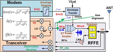
Figure 8. 4G/5G I & Q transmitter diagram.
The intermodulation distortion (IMD) introduced by the delay mismatch for a polar system is given by:
where BRF is the BW of the RF signal and ![]() ${\Delta _\tau }$ is the delay mismatch. The
${\Delta _\tau }$ is the delay mismatch. The ![]() ${\Delta _\tau }$ minimum between left and right IMD determines the adjacent channel leakage ratio (ACLR) of the ET PA and tracker:
${\Delta _\tau }$ minimum between left and right IMD determines the adjacent channel leakage ratio (ACLR) of the ET PA and tracker:
where k is a correction factor determined by RF signal peak-to-average power ratio (PAPR) and how much the PA is compressed. 5G NR signals can reach a 10.5 dB PAPR. For linear polar modulation, the driver might be compressed and therefore is very challenging to get the right linearity compared with an ET system using a I & Q modulator, a class E PA, and an envelope signal with a basic look-up shaping table using several points. This solution is simpler than using a load modulation Doherty PA with phase/gain DPD. As the output power and BW for 5G continue to increase, operating the ET becomes more challenging for modulation BWs exceeding 100 MHz. A new envelope-controlled class E PA structure is proposed and presented in Fig. 9 from this perspective.
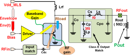
Figure 9. Input enveloped-controlled class E power amplifier.
The PA maximum output power Pout, considering low RF losses in the output match, is given by:
 \begin{equation}{P_{out}} = k \cdot \frac{{{{(Vdd - Vkn)}^2}}}{{{R_{load}}}}\end{equation}
where Vdd is the PA voltage supply, Vkn is the knee voltage, and Rload is the load line. For class E PAs k = 1.365 and for class B k = 0.5. In ET mode Vdd is dynamically modulated with the envelope using an ET PMIC.
To enhance the efficiency of high PAPR 4G/5G transmit (Tx) signals, other techniques have been developed such as dynamic load modulation (DLM), which includes varactor DLM and active load modulation (ALM). ALM utilize active current injection to tune the load as in Chirex out-phasing PA, Doherty PAs and load modulated balanced amplifier [Reference Pednekar, Hallberg, Fager and Barton27]. The PA load line Rload is determined mainly by how much current conduction can provide the output transistor. Based on this observation a new envelope-controlled bias PA technique is proposed, as presented in Figs. 9 and 10. The identical envelope signal can be also applied to Vdd line. However, in this scenario, it may require a separate delay calibration or the implementation of multiple level supply control.

Figure 10. Input enveloped-controlled class E CMOS/SOI differential power amplifier.
The bias driver is connected to the PA core through an RF isolation inductor Lg. The identical schematic concept can be used for a differential PA structure, in such case the input balun provides the required DC isolation (Fig. 10). The servo amplifier used in the bias structure incorporates a current feedback architecture to improve both the frequency response and slew rate, as illustrated in Fig. 11. Vbias_PA supplies the bias for PA, which can be a CMOS or SOI PA for FR2. The feedback signal Ibias_PA is utilized to sense the output PA current, providing both precise bias and tracking for ET.
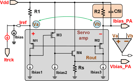
Figure 11. Current feedback servo amplifier structure.
Thermal management for RFFE modules
Thermal management of RF power circuits is an essential part of design approach to guarantee RF performances in all operating conditions and avoiding circuits degradation and failure. This becomes even more critical with increased number of PA operating simultaneously, e.g., for 5G there might be three PAs turned on at a time. One of the primary concerns preventing the deployment of SOI technology for PAs in 5G FR1 RFFE is the thermal management. The increase in power delivered to the antenna, reaching up to 26 dBm for high-power user equipment [Reference Pehlke, Brunel, Walsh and Kovacic4, Reference Balteanu24] has made this issue even more crucial. A simple schematic for monitoring the temperature used in current smartphone application is presented in Fig. 12. The analogue value for temperature Vtemp is used to feed the Ibias circuitry and determine the right profile; typically increasing the LNA/PA bias current with the temperature. To obtain an accurate temperature profile, multiple sensors are placed on the CMOS/SOI dies (pn diodes). Additionally, the temperature is digitized and transmitted to the modem via a MIPI RFFE at a speed of maximum 52 MHz. The standard maximum margin of error for this architecture is ±4°C at 120°C. Vtemp is determined by the equation:
 \begin{equation}Vtemp = Vcal \cdot (\frac{{Rf}}{{Rin}} + 1) - Vd \cdot \frac{{Rf}}{{Rin}}\end{equation}
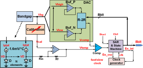
Figure 12. RFFE thermal monitor circuitry.
where Vcal is the calibration voltage and Vd is the diode voltage. Through calibration all the offsets as well diode voltage variations are cancelled.
The thermal monitor can operate with a fast clock (e.g., 1–5 MHz), as well with a slow clock (25 KHz) to reduce the RF spurs during measurement activity. The thermal monitor can use N elements to map the temperature on a single semiconductor die, especially if there are PAs integrated on the die.
Acoustic filters
The transition from 3G/4G to 5G, with requirements for different RF transmitters coexistence, drives the use of several acoustic filters. For lower frequencies, up to 2 GHz, the filter requirements have been handled using surface acoustic wave (SAW) filters (Fig. 13). With the evolution to 5G and more high and ultra-high bands RFFEs [Reference Balteanu, Modi, Choi, Lee, Drogi and Khesbak28], there is a high demand for bulk acoustic wave (BAW) filters and the most used is the film bulk acoustic resonator (FBAR).
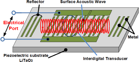
Figure 13. SAW filter structure.
To prevent the acoustic waves from dissipating into silicon substrate, an acoustic Bragg reflector is manufactured using thin layer, as seen in solidly mounted resonator BAW. Another approach etches a cavity underneath the active area as in FBAR shown in Fig. 14. Both types of BAW filters have quality factors ranging from 3000 to 4000 (higher than those of SAW filters). However, there are promising results with comparable quality factors for the new lithium tantalate bonded to silicon hybrid substrate silicon SAW [Reference Ruby, Gilbert, Lee, Nilchi and Kim29].
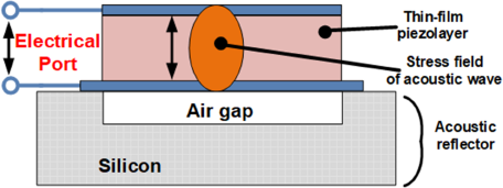
Figure 14. FBAR acoustic filter structure.
One of the most used 5G band by the cellular operators is the TDD band n41 (2469–2690 MHz), with the FBAR frequency response insertion loss (IL) for this band shown in Fig. 15. In-band ripple of the acoustic filter affects the ET delay calibration. To mitigate in-band ripple, an average delay calibration is required which slows down the calibration time.
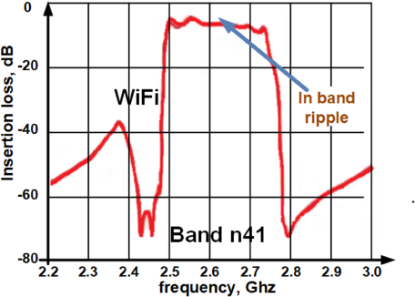
Figure 15. FBAR filter response for band n41.
The filter has also higher IL at band edges, and this makes difficult to achieve an ACLR lower than −35 dBc (with DPD) at the low side edge of the n41 filter to minimize the emissions in WiFi channels as shown in Fig. 16 for a 5G PA with 100 MHz modulation BW and with an output power of 26 dBm.

Figure 16. Band n41 PA and BAW filter under ET operation.
Antenna tuners
Current smartphones use several antennas to achieve high DRs through techniques such as CA, MIMO, WiFi with MIMO. Most smartphones are equipped with eight to nine antennas for optimal performance. Utilizing optimal impedance matching and propagation path, the switching between antennas is achieved with high linearity switches to maximize SINR. This is one of several diversity schemes utilized to enhance the quality and dependability of the RF wireless connection to the base station. Each antenna covers several bands, and for these reasons ATs are used together with ITs to correct the antenna mismatch as presented in Fig. 17. While signals in lower frequency bands have the capability to propagate over long distances and penetrate building with ease, mmWave FR2 signals have a shorter range and do not penetrate solid materials efficiently. Additionally implementing beamforming for mmWave FR2 is more complex than utilizing antenna tuners for bands under 6 GHz [Reference Balteanu24].
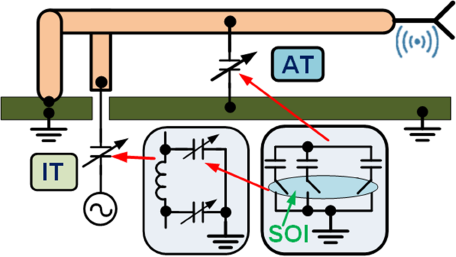
Figure 17. Antenna and impedance tuners.
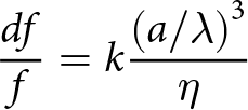
Antenna BW is given by the formula:
 \begin{equation}\frac{{df}}{f} = k\frac{{{{(a/\lambda )}^3}}}{\eta }\end{equation}
where a is antenna length, λ is the wavelength, η is the antenna radiation efficiency, and f is frequency. From equation (6) covering wider bands can be obtained using larger antennas or lower radiation efficiency which both are undesirable and explain the need of using antenna tuners. Figure 18 presents the antenna efficiency after tuning for an LB antenna.
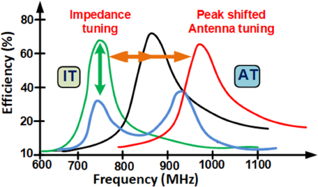
Figure 18. Antenna and impedance tuners response.
To tune the antenna, a coupler is required to be used as shown in Fig. 19 as positioned before the tuner (Cp3). Typically, a coupler has approximatively 0.2 dB RF IL and adds to the power loss. For Cp3 position, the coupler can be used for ET delay calibration [Reference Balteanu, Zhu and DiCarlo26]. If a full DPD is required to correct the ACLR, the best coupler position is Cp1. While position Cp2 may result in less error in RF power measurement within the band when implementing full DPD, it does not offer as effective ACLR correction.

Figure 19. Sub-6 GHZ RFFE coupler positioning.
Implementation and measurements
The gallium arsenide (GaAs) heterojunction bipolar transistor PA, ET driver amplifier together with RF SOI switches and RF FBAR filters are integrated on the same substrate in a multi-chip module (MCM). For current FR1 smartphones and 6 GHz RFFE, the ET circuit is connected to the modem via a differential analogue signal Env(t). This interface follows the MIPI ET standard and is known as the eTrackSM [Reference Balteanu12]. Figure 20 presents the interface for the envelope signal Env(t), utilized in the control of a class E PA, based on the proposed concept.
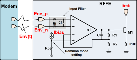
Figure 20. Envelope input circuit.
The detailed schematic for transconductor circuit a1 is presented in Fig. 21. Typically, the input voltage levels can reach 1.4 V peak to peak and therefore there is no need of additional gain which will add noise into the ET system. The interface standard has been initially defined to work up to 20 MHz, however it is used currently to operate up to 150 MHz for 5G applications. As the modulation BW increases, a new interface between the modem and ET becomes necessary. This interface must be capable of operating up to 2 GHz. A promising solution is the MIPI-PHY [Reference Lancheres and Hafed30] protocol.
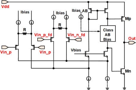
Figure 21. Envelope input circuit – transconductor detail.
The ET signal, Env(t), is a differential signal designed to eliminate common mode noise and prevent interference from other signals. Ibias from Fig. 20 sets the desired common mode voltage for the ET interface. The control circuit for the ET presented is implemented using a 0.18 µm CMOS technology and is designed to control a push pull class E GaAs PA, as presented in Fig. 22.
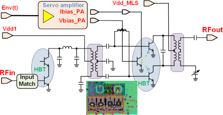
Figure 22. GaAs push-pull power amplifier.
The PA bias current Ibias_PA is determined by the formula:
 \begin{equation}Ibias\_PA = (Itrck + Ibias) \cdot \frac{{R1}}{{R2}}\end{equation}
where Itrck is providing the tracking (for ET) and Ibias has a proportional with temperature dependent (PTAT) characteristic profile. In FR1 space applications, the ET is only utilized for the final stage, as there are delays in the RF signal between stage 1 and 2 of the PA.
One of challenges in PA control is maintaining consistent behavior of PA across varying temperature, especially in TDD systems. For this reason, Ibias presented in Fig. 10 is proportional with the temperature based on different slopes and the CMOS die sits on GaAs die. This allows for precise temperature sensing of the PA temperature, as depicted for a Mead Band (MB) RFFE in Fig. 23.
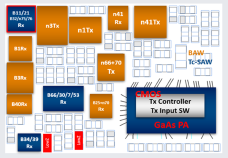
Figure 23. MB RFFE component placement.
For two of 5G bands n41 (FDD Tx 1710–1780 MHz) and n66 (TDD 2496–2290 MHz) the measured performance using an envelope-controlled class E PA is presented in Table 1.
Table 1. Measurements for 5G bands n66 and n41

The ACLR is measured using a simple ET look-up table and without DPD; using DPD the ACLR is expected to drop to −45 dBc. For a lower ACLR, without using DPD, the PA added efficiency (PAE) drops to 39% from 42% to 45%, for a minimum gain of 27 dB. As the number of 5G users continues to rise, there is a growing demand for improved 5G network performance. An important metric in evaluating the reliability of a 5G network is the adjacent channel interference ratio (ACIR), which measures the total leakage between two transmitters. This leakage is determined by both the ACLR and adjacent channel selectivity, as defined by:
 \begin{equation}ACIR = \tfrac{1}{{\frac{1}{{ACLR}} + \frac{1}{{ACS}}}}\end{equation}
To improve the ACIR, it is necessary to achieve an ACLR higher than −38 dBc, ideally reaching levels as low as −45 dBc using ET and DPD techniques.
The suggested concept of envelope-controlled PA amplifier is applicable for implementation of FR2 mmWave PAs as well. The architecture in Fig. 24 requires a total of three stages to achieve a minimum gain of 26 dB for the Tx PA and Rx LNA in the FR2 5G bands n257–n263.
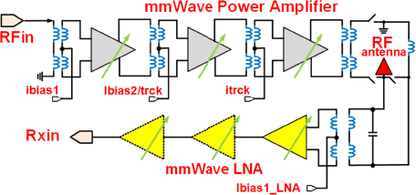
Figure 24. 5G FR2 PA/LNA schematic.
The ET tracking for FR1 is limited to the last PA stage, while for FR2 it can track the last two stages. Therefore, all bias circuits shown in Fig. 10 are identical to accommodate this implementation as well different modulation BW. One main challenge for FR2 versus FR1 is the calibration procedure involving the bias currents. The RF gain and power are not primarily influenced by the Ibias, in comparison to FR1. The variation in RF gain and power is also affected by a mismatch in local components. Accurate calibration of bias currents for FR2 can be achieved by utilizing precise RF peak detectors to measure and optimize the RF gain.
From this perspective the calibration as well temperature compensation in real time is more complicated as in FR1. Also, for FR2 the modulation BW is increased from 100–150 MHz to 1 GHz. An FR2 layout amplifier for 5G band n262 (47.2–48.2 GHz) implemented in a 45 nm SOI technology is presented in Fig. 25. The total area for n262 PA is 0.218 mm2.
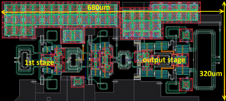
Figure 25. 5G FR2 band n262 layout.
The beamforming system utilizes 4/8 integrated PAs on single die. The measured average RF power of one PA operating at 64QAM/200 MHz is 10 dBm, with an EVM of −33.5%. By implementing a basic DPD technique, the EVM improves to a minimum of −36%. One of the limitations for high modulation BW (over 200 MHz) is related to PA thermal behavior. To overcome this, the implementation uses local temperature detection and compensation circuitry. Utilizing local tracking via bias currents offers a more digital approach to ET for FR2 application, as illustrated in Fig. 26. An envelope-controlled ET approach can use the same look-up table for beamforming. A similar approach with a single look-up table was proposed in paper [Reference Okada21], using Doherty PAs.
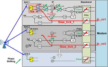
Figure 26. 5G FR2 beam forming and Ibias with ET control.
For FR2 and high modulation BW the approach of using an observation receiver is not practical and therefore a new method of using precise RF detectors is proposed. The peak/rms detector (Fig. 27) is integrated on the same SOI/CMOS die and connected through a coupler to the PA output. M2 provides the bias, while M1a and RF filter Rd and Cf perform the detection. Similarly, M1b and Rd generate a replica bias with a comparable DC voltage to that of M1a and Rd. The source followers M3 and M4 isolate the RF detection and serve as the interface for the postprocessing circuitry.
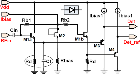
Figure 27. 5G FR1/FR2 power detector.
The FR2 SOI die uses several RF peak/rms detectors across the die, and they use a single analogue postprocessing circuitry, which interfaces with the transceiver/modem, as shown in Fig. 28. Vcal pin is utilized for calibration of the RF detectors in absence of RF signal.
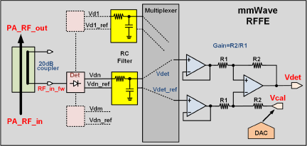
Figure 28. 5G FR1/FR2 power detector analogue postprocessing circuitry.
The measured RF detector shows a precision of 0.1 dB with less than 0.01 dB flatness in band which is more than enough to accommodate the FBAR ripple for TDD band n41 (2.469–2.690 GHz) when the RF detector is used as RF calibration sensor. The RF detector retains its high precision across process variation for FR2 frequencies, as presented in Fig. 29 for band n262.
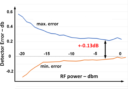
Figure 29. 5G FR2 band n262 power detector error under process variation.
Furthermore, the RF detector has a broadband response and the measured time response for 5G FR2 band n262 (48 GHz) is less than 100 ns, as presented in Fig. 30. If the modulation BW for 5G signal is higher (such as 1–2 GHz), the time response can be adjusted through post-detection low-pass RC filters.

Figure 30. 5G FR2 band n262 power detector time response for CW RF signals.
The implementation of a fast and accurate RF peak/rms detector for ET and power calibration (Fig. 31) simplifies the calibration structure and takes advantage of the progress in semiconductor technologies, particularly in small feature size, for modern 3 nm/5 nm FinFET technologies. This approach is more straightforward when compared to the current ET calibration of smartphones [Reference Balteanu, Pingale, Thoomu and Choi31], which utilize observation receivers. The calibration process involves utilizing a slow modulating RF waveform with two RF peak signals, where calibration is achieved when RF detectors detects equal values for both peaks. The principle closely resembles that of [Reference Balteanu, Zhu and DiCarlo26] but eliminates the use of impractical observation receivers at FR2 frequencies.
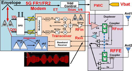
Figure 31. 5G ET and power calibration schematic architecture.
Conclusions
The smartphone industry is a very large and constantly evolving market, where changes in hardware and architecture must undergo extensive validation before being implemented. Despite the introduction of new mobile device models every year, this process takes a significant amount of time. The recent shift from 4G to 5G technology was relatively swift, but it is anticipated that the next major transition to 6G will take longer before full deployment. As such, it is crucial for the cellular industry to diversify its applications and learn from the challenges faced during slow deployment of 5G FR2.
To address some of these issues, this paper proposes a RF PA architecture utilizing an envelope-controlled PA and RF ET, as well as precise RF detectors for transmit power calibration. This design has the capability to handle a modulation BW of 2 GHz and support FR2 frequencies. These circuits are currently used for low modulation BW applications on existing mobile devices, but they also pave the way for seamless integration into future generation of RF technologies such as 5G+ and 6G, along with other mobile transmitters.
Competing interests
The author declares none.

Florinel Balteanu received the M.S. degree in electrical engineering from Polytechnic Institute, Bucharest, Romania, in 1983, and the Ph.D. degree in electrical engineering from Transylvania University, Brasov, Romania, in 1995. From 1983 to 1992, he was with the Institute of Nuclear Research, Pitesti, Romania, working on electronic instrumentation for nuclear power reactors. In 1993, he joined the Department of Electronics, University of Pitesti, Romania, as an Assistant Professor doing research in analogue circuits. From 1992 to 1993, he was a Fulbright Visiting Scholar at the Centre for Reliable Computing, Stanford University, Stanford, CA. In 1996, he joined Philsar Semiconductor, Ottawa, ON, Canada, as a Senior ASIC Designer, a company later acquired by Conexant Systems, Inc. (now known as Skyworks Solutions, Inc.). His work has been focused on the design of radio circuits for GPS receivers, Bluetooth transceivers, and GSM/CDMA cellular transceivers. He is presently a Technical Director with Skyworks Solutions Inc., Irvine, CA and is involved in designing circuits for Envelope Tracking and Front-End Modules in CMOS and SOI CMOS. He presented short courses and tutorials as an Invited Speaker at IEEE Microwave Theory and Techniques Society (MTT-S) International Microwave Symposium (IMS). European Microwave Week (EuMW), European Solid-State Circuits Conference (ESSCIRC) and Asia-Pacific Microwave Conference (APMC). He holds 98 U.S. patents, with several more pending. He is the author of the chapter “Envelope Tracking Techniques” in the IET book “Radio Frequency and Microwave Power Amplifiers, Vol. 2: Efficiency and Linearity”.


