Hostname: page-component-745bb68f8f-s22k5 Total loading time: 0 Render date: 2025-01-28T11:41:26.495Z Has data issue: false hasContentIssue false

Grain size dependence of the twin length fraction in nanocrystalline Cu thin films via transmission electron microscopy based orientation mapping

Published online by Cambridge University Press:  10 February 2015
Xuan Liu*
Affiliation:
Department of Materials Science and Engineering, Carnegie Mellon University, Pittsburgh, Pennsylvania 15213, USA
Noel T. Nuhfer
Affiliation:
Department of Materials Science and Engineering, Carnegie Mellon University, Pittsburgh, Pennsylvania 15213, USA
Andrew P. Warren
Affiliation:
Department of Materials Science and Engineering, University of Central Florida, Orlando, Florida 32816, USA
Kevin R. Coffey
Affiliation:
Department of Materials Science and Engineering, University of Central Florida, Orlando, Florida 32816, USA
Gregory S. Rohrer
Affiliation:
Department of Materials Science and Engineering, Carnegie Mellon University, Pittsburgh, Pennsylvania 15213, USA
Katayun Barmak*
Affiliation:
Department of Applied Physics and Applied Mathematics, Columbia University, New York, NY 10027, USA
*
a)Address all correspondence to this author. e-mail: kb2612@columbia.edu
Get access

Abstract

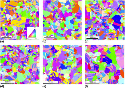
Transmission electron microscopy (TEM) based orientation mapping has been used to measure the length fraction of coherent and incoherent Σ3 grain boundaries in a series of six nanocrystalline Cu thin films with thicknesses in the range of 26–111 nm and grain sizes from 51 to 315 nm. The films were annealed at the same temperature (600 °C) for the same length of time (30 min), have random texture, and vary only in grain size and film thickness. A strong grain size dependence of Σ3 (coherent and incoherent) and coherent Σ3 boundary fraction was observed. The experimental results are quantitatively compared with three physical models for the formation of annealing twins developed for microscale materials. The experimental results for the nanoscale Cu films are found to be in good agreement with the two microscale models that explain twin formation as a growth accident process.

Type
Articles
Copyright
Copyright © Materials Research Society 2015 

Access options

Get access to the full version of this content by using one of the access options below. (Log in options will check for institutional or personal access. Content may require purchase if you do not have access.)

References

REFERENCES

Sun, T., Yao, B., Warren, A.P., Barmak, K., Toney, M.F., Peale, R.E., and Coffey, K.R.: Surface and grain-boundary scattering in nanometric Cu films. Phys. Rev. B 81, 155454 (2010).Google Scholar
Lu, L., Shen, Y.F., Chen, X.H., Qian, L.H., and Lu, K.: Ultrahigh strength and high electrical conductivity in copper. Science 304, 422 (2004).CrossRefGoogle ScholarPubMed
Lin, P., Palumbo, G., Erb, U., and Aust, K.: Influence of grain boundary character distribution on sensitization and intergranular corrosion of alloy 600. Scr. Metall. Mater. 33, 1387 (1995).Google Scholar
Lee, S.B., Key, T.S., Liang, Z., Garcia, R.E., Wang, S., Tricoche, X., Rohrer, G.S., Saito, Y., Ito, C., and Tani, T.: Microstructure design of lead-free piezoelectric ceramics. J. Eur. Ceram. Soc. 33, 313 (2013).Google Scholar
Watanabe, T.: An approach to grain boundary design for strong and ductile polycrystals. Res Mech. 11, 47 (1984).Google Scholar
Field, D., Bradford, L., Nowell, M., and Lillo, T.: The role of annealing twins during recrystallization of Cu. Acta Mater. 55, 4233 (2007).CrossRefGoogle Scholar
Randle, V.: Twinning-related grain boundary engineering. Acta Mater. 52, 4067 (2004).Google Scholar
Fuchs, K.: The conductivity of thin metallic films according to the electron theory of metals. Proc. Cambridge Philos. Soc. 34, 100 (1938).Google Scholar
Shen, Y., Lu, L., Lu, Q., Jin, Z., and Lu, K.: Tensile properties of copper with nano-scale twins. Scr. Mater. 52, 989 (2005).Google Scholar
Anderoglu, O., Misra, A., Wang, H., and Zhang, X.: Thermal stability of sputtered Cu films with nanoscale growth twins. J. Appl. Phys. 103, 094322 (2008).Google Scholar
Chen, K.C., Wu, W.W., Liao, C.N., Chen, L.J., and Tu, K.N.: Observation of atomic diffusion at twin-modified grain boundaries in copper. Science 321, 1066 (2008).Google Scholar
Sutton, A.P. and Balluffi, R.W.: Interfaces in crystalline materials. (Clarendon Press, New York, NY, 1995); pp. 295.Google Scholar
Xu, D., Sriram, V., Ozolins, V., Yang, J-M., Tu, K., Stafford, G.R., Beauchamp, C., Zienert, I., Geisler, H., and Hofmann, P.: Nanotwin formation and its physical properties and effect on reliability of copper interconnects. Microelectron. Eng. 85, 2155 (2008).CrossRefGoogle Scholar
Kohama, K., Ito, K., Matsumoto, T., Shirai, Y., and Murakami, M.: Role of Cu film texture in grain growth correlated with twin boundary formation. Acta Mater. 60, 588 (2012).Google Scholar
Park, N-J. and Field, D.: Predicting thickness dependent twin boundary formation in sputtered Cu films. Scr. Mater. 54, 999 (2006).CrossRefGoogle Scholar
Pantleon, K., Gholinia, A., and Somers, M.A.: Quantitative microstructure characterization of self-annealed copper films with electron backscatter diffraction. Phys. Status Solidi A 205, 275 (2008).Google Scholar
Rauch, E.F. and Dupuy, L.: Rapid spot diffraction patterns identification through template matching. Arch. Metall. Mater. 50, 87 (2005).Google Scholar
Rauch, E.F. and Veron, M.: Coupled microstructural observations and local texture measurements with an automated crystallographic orientation mapping tool attached to a tem. Materialwiss. Werkstofftech. 36, 552 (2005).Google Scholar
Rauch, E.F., Portillo, J., Nicolopoulos, S., Bultreys, D., Rouvimov, S., and Moeck, P.: Automated nanocrystal orientation and phase mapping in the transmission electron microscope on the basis of precession electron diffraction. Z. Kristallogr. 225, 103 (2010).CrossRefGoogle Scholar
Darbal, A.D., Ganesh, K.J., Liu, X., Lee, S.B., Ledonne, J., Sun, T., Yao, B., Warren, A.P., Rohrer, G.S., Rollett, A.D., Ferreira, P.J., Coffey, K.R., and Barmak, K.: Grain boundary character distribution of nanocrystalline Cu thin films using stereological analysis of transmission electron microscope orientation maps. Microsc. Microanal. 19, 111 (2013).Google Scholar
Carpenter, J.S., Liu, X., Darbal, A., Nuhfer, N.T., McCabe, R.J., Vogel, S.C., LeDonne, J.E., Rollett, A.D., Barmak, K., Beyerlein, I.J., and Mara, N.A.: A comparison of texture results obtained using precession electron diffraction and neutron diffraction methods at diminishing length scales in ordered bimetallic nanolamellar composites. Scr. Mater. 67, 336 (2012).CrossRefGoogle Scholar
Liu, X., Nuhfer, T., Ledonne, J., Lee, S., Rollett, A., Barmak, K., Carpenter, J., and Darbal, A.: Precession-assisted nanoscale phase and crystal orientation mapping of Cu-Nb composites in the transmission electron microscope. Microsc. Microanal. 18, 1426 (2012).Google Scholar
Liu, X., Nuhfer, N., Rollett, A., Sinha, S., Lee, S-B., Carpenter, J., LeDonne, J., Darbal, A., and Barmak, K.: Interfacial orientation and misorientation relationships in nanolamellar Cu/Nb composites using transmission-electron-microscope-based orientation and phase mapping. Acta Mater. 64, 333 (2014).CrossRefGoogle Scholar
Liu, X., Choi, D., Beladi, H., Nuhfer, N.T., Rohrer, G.S., and Barmak, K.: The five parameter grain boundary character distribution of nanocrystalline tungsten. Scr. Mater. 69, 413 (2013).CrossRefGoogle Scholar
Gleiter, H.: Formation of annealing twins. Acta Metall. 17, 1421 (1969).CrossRefGoogle Scholar
Mahajan, S., Pande, C., Imam, M., and Rath, B.: Formation of annealing twins in fcc crystals. Acta Mater. 45, 2633 (1997).CrossRefGoogle Scholar
Burgers, W.: Stimulation crystals and twin-formation in recrystallized aluminium. Nature 157, 76 (1946).CrossRefGoogle Scholar
Burgers, W.: Crystal growth in the solid state (recrystallization). Physica 15, 92 (1949).Google Scholar
Burgers, W., Meijs, J., and Tiedema, T.: Frequency of annealing twins in copper crystals grown by recrystallization. Acta Metall. 1, 75 (1953).CrossRefGoogle Scholar
Dash, S. and Brown, N.: An investigation of the origin and growth of annealing twins. Acta Metall. 11, 1067 (1963).CrossRefGoogle Scholar
Kopezky, C.V., Novikov, V.Y., Fionova, L., and Bolshakova, N.: Investigation of annealing twins in fcc metals. Acta Metall. 33, 873 (1985).Google Scholar
Kopezky, C.V., Andreeva, A.V., and Sukhomlin, G.D.: Multiple twinning and specific properties of sigma = 3N boundaries in FCC crystals. Acta Metall. Mater. 39, 1603 (1991).Google Scholar
Pande, C., Imam, M., and Rath, B.: Study of annealing twins in fcc metals and alloys. Metall. Trans. A 21, 2891 (1990).CrossRefGoogle Scholar
Chen, F. and Gardner, D.: Influence of line dimensions on the resistance of Cu interconnections. IEEE Electron Device Lett. 19, 508 (1998).Google Scholar
Sun, T., Yao, B., Warren, A.P., Kumar, V., Roberts, S., Barmak, K., and Coffey, K.R.: Classical size effect in oxide-encapsulated Cu thin films: Impact of grain boundaries versus surfaces on resistivity. J. Vac. Sci. Technol., A 26, 605 (2008).CrossRefGoogle Scholar
Yao, B., Petrova, R.V., Vanfleet, R.R., and Coffey, K.R.: A modified back-etch method for preparation of plan-view high-resolution transmission electron microscopy samples. J. Electron Microsc. 55, 209 (2006).CrossRefGoogle ScholarPubMed
Wright, S.I. and Larsen, R.J.: Extracting twins from orientation imaging microscopy scan data. J. Microsc. 205, 245 (2002).Google Scholar
Rohrer, G.S., Saylor, D.M., El-Dasher, B., Adams, B.L., Rollett, A.D., and Wynblatt, P.: The distribution of internal interfaces in polycrystals. Z. Metallkd. 95, 197 (2004).CrossRefGoogle Scholar
Barmak, K., Eggeling, E., Emelianenko, M., Epshteyn, Y., Kinderlehrer, D., Sharp, R., and Ta'asan, S.: Critical events, entropy, and the grain boundary character distribution. Phys. Rev. B 83, 134117:112 (2011).CrossRefGoogle Scholar
Rohrer, G.S.: Grain boundary energy anisotropy: A review. J. Mater. Sci. 46, 5881 (2011).Google Scholar
Holm, E.A., Olmsted, D.L., and Foiles, S.M.: Comparing grain boundary energies in face-centered cubic metals: Al, Au, Cu and Ni. Scr. Mater. 63, 905 (2010).CrossRefGoogle Scholar
Mackenzie, J.K., Moore, A.J.W., and Nicholas, J.F.: Bonds broken at atomically flat crystal surface—1: face-centered and body-centered cubic crystals. J. Phys. Chem. Solids 23, 185 (1962).CrossRefGoogle Scholar
Rohrer, G.S., Holm, E.A., Rollett, A.D., Foiles, S.M., Li, J., and Olmsted, D.L.: Comparing calculated and measured grain boundary energies in nickel. Acta Mater. 58, 5063 (2010).CrossRefGoogle Scholar
Holm, E.A., Rohrer, G.S., Foiles, S.M., Rollett, A.D., Miller, H.M., and Olmsted, D.L.: Validating computed grain boundary energies in fcc metals using the grain boundary character distribution. Acta Mater. 59, 5250 (2011).Google Scholar
Beladi, H. and Rohrer, G.S.: The relative grain boundary area and energy distributions in a ferritic steel determined from three-dimensional electron backscatter diffraction maps. Acta Mater. 61, 1404 (2013).CrossRefGoogle Scholar
Beladi, H. and Rohrer, G.S.: The distribution of grain boundary planes in interstitial free steel. Metall. Mater. Trans. A 44A, 115 (2013).CrossRefGoogle Scholar
Li, Q., Cahoon, J.R., and Richards, N.L.: On the calculation of annealing twin density. Scr. Mater. 55, 1155 (2006).Google Scholar
Meyers, M.A. and Murr, L.E.: A model for the formation of annealing twins in FCC metals and alloys. Acta Metall. 26, 951 (1978).Google Scholar
Warrington, D.H. and Boon, M.: Ordered structures in random grain-boundaries; some geometrical probabilities. Acta Metall. 23, 599 (1975).Google Scholar
Carpenter, D.T., Rickman, J.M., and Barmak, K.: A methodology for automated quantitative microstructural analysis of transmission electron micrographs. J. Appl. Phys. 84, 5843 (1998).Google Scholar