Hostname: page-component-cd9895bd7-gvvz8 Total loading time: 0 Render date: 2024-12-27T13:29:40.336Z Has data issue: false hasContentIssue false

Manufacturing strategies for wafer-scale two-dimensional transition metal dichalcogenide heterolayers

Published online by Cambridge University Press:  05 February 2020

Mengjing Wang
Affiliation:
NanoScience Technology Center, University of Central Florida, Orlando, Florida 32826, USA
Hao Li
Affiliation:
NanoScience Technology Center, University of Central Florida, Orlando, Florida 32826, USA; and Department of Materials Science and Engineering, University of Central Florida, Orlando, Florida 32826, USA
Tae-Jun Ko
Affiliation:
NanoScience Technology Center, University of Central Florida, Orlando, Florida 32826, USA
Mashiyat Sumaiya Shawkat
Affiliation:
NanoScience Technology Center, University of Central Florida, Orlando, Florida 32826, USA; and Department of Electrical and Computer Engineering, University of Central Florida, Orlando, Florida 32816, USA
Emmanuel Okogbue
Affiliation:
NanoScience Technology Center, University of Central Florida, Orlando, Florida 32826, USA; and Department of Electrical and Computer Engineering, University of Central Florida, Orlando, Florida 32816, USA
Changhyeon Yoo
Affiliation:
NanoScience Technology Center, University of Central Florida, Orlando, Florida 32826, USA
Sang Sub Han
Affiliation:
NanoScience Technology Center, University of Central Florida, Orlando, Florida 32826, USA; and Department of Materials Science and Engineering, Seoul National University, Seoul 08826, South Korea
Md Ashraful Islam
Affiliation:
NanoScience Technology Center, University of Central Florida, Orlando, Florida 32826, USA; and Department of Electrical and Computer Engineering, University of Central Florida, Orlando, Florida 32816, USA
Kyu Hwan Oh
Affiliation:
Department of Materials Science and Engineering, Seoul National University, Seoul 08826, South Korea
Yeonwoong Jung*
Affiliation:
NanoScience Technology Center, University of Central Florida, Orlando, Florida 32826, USA; Department of Materials Science and Engineering, University of Central Florida, Orlando, Florida 32826, USA; and Department of Electrical and Computer Engineering, University of Central Florida, Orlando, Florida 32816, USA
*
a)Address all correspondence to this author. e-mail: yeonwoong.jung@ucf.edu
Get access

Abstract

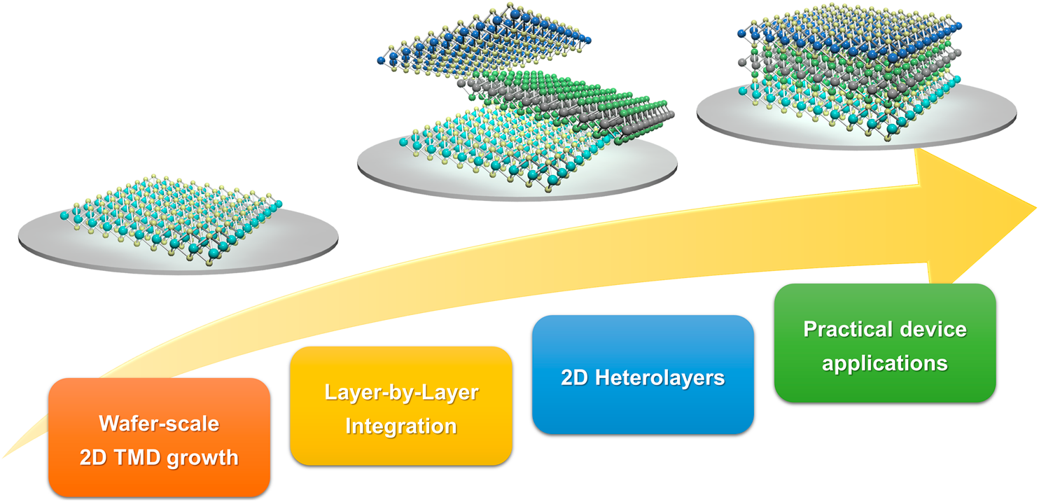
Modern electronics have been geared toward exploring novel electronic materials that can encompass a broad set of unusual functionalities absent in conventional platforms. In this regard, two-dimensional (2D) transition metal dichalcogenide (TMD) semiconductors are highly promising, owing to their large mechanical resilience coupled with superior transport properties and van der Waals (vdW) attraction-enabled relaxed assembly. Moreover, 2D TMD heterolayers based on chemically distinct constituent layers exhibit even more intriguing properties beyond their mono-component counterparts, which can materialize only when they are manufactured on a technologically practical wafer-scale. This mini-review provides a comprehensive overview of recent progress in exploring wafer-scale 2D TMD heterolayers of various kinds. It extensively surveys a variety of manufacturing strategies and discusses their scientific working principles, resulting 2D TMD heterolayers, their material properties, and device applications. Moreover, it offers extended discussion on remaining challenges and future outlooks toward further improving the material quality of 2D TMD heterolayers in both material and manufacturing aspects.

Type
Invited Feature Paper - Review
Copyright
Copyright © Materials Research Society 2020

Access options

Get access to the full version of this content by using one of the access options below. (Log in options will check for institutional or personal access. Content may require purchase if you do not have access.)

Footnotes

This paper has been selected as an Invited Feature Paper.

References

Gooding, J.J.: Nanostructuring electrodes with carbon nanotubes: A review on electrochemistry and applications for sensing. Electrochim. Acta 50, 3049 (2005).CrossRefGoogle Scholar
Li, Y., Qian, F., Xiang, J., and Lieber, C.M.: Nanowire electronic and optoelectronic devices. Mater. Today 9, 18 (2006).CrossRefGoogle Scholar
Trojanowicz, M.: Analytical applications of carbon nanotubes: A review. TrAC, Trends Anal. Chem. 25, 480 (2006).CrossRefGoogle Scholar
Allen, M.J., Tung, V.C., and Kaner, R.B.: Honeycomb carbon: A review of graphene. Chem. Rev. 110, 132 (2009).CrossRefGoogle Scholar
Zhang, Y., Zhang, L., and Zhou, C.: Review of chemical vapor deposition of graphene and related applications. Acc. Chem. Res. 46, 2329 (2013).CrossRefGoogle ScholarPubMed
Bhimanapati, G.R., Lin, Z., Meunier, V., Jung, Y., Cha, J., Das, S., Xiao, D., Son, Y., Strano, M.S., and Cooper, V.R.: Recent advances in two-dimensional materials beyond graphene. ACS Nano 9, 11509 (2015).CrossRefGoogle ScholarPubMed
Tan, C., Cao, X., Wu, X-J., He, Q., Yang, J., Zhang, X., Chen, J., Zhao, W., Han, S., and Nam, G-H.: Recent advances in ultrathin two-dimensional nanomaterials. Chem. Rev. 117, 6225 (2017).CrossRefGoogle ScholarPubMed
Zhang, H.: Ultrathin two-dimensional nanomaterials. ACS Nano 9, 9451 (2015).CrossRefGoogle ScholarPubMed
Das, S., Robinson, J.A., Dubey, M., Terrones, H., and Terrones, M.: Beyond graphene: Progress in novel two-dimensional materials and van der Waals solids. Annu. Rev. Mater. Res. 45, 1 (2015).CrossRefGoogle Scholar
Wang, F., Wang, Z., Wang, Q., Wang, F., Yin, L., Xu, K., Huang, Y., and He, J.: Synthesis, properties and applications of 2D non-graphene materials. Nanotechnology 26, 292001 (2015).CrossRefGoogle ScholarPubMed
Mak, K.F., Lee, C., Hone, J., Shan, J., and Heinz, T.F.: Atomically thin MoS2: A new direct-gap semiconductor. Phys. Rev. Lett. 105, 136805 (2010).CrossRefGoogle Scholar
Conley, H.J., Wang, B., Ziegler, J.I., Haglund, R.F. Jr., Pantelides, S.T., and Bolotin, K.I.: Bandgap engineering of strained monolayer and bilayer MoS2. Nano Lett. 13, 3626 (2013).CrossRefGoogle ScholarPubMed
Susarla, S., Kutana, A., Hachtel, J.A., Kochat, V., Apte, A., Vajtai, R., Idrobo, J.C., Yakobson, B.I., Tiwary, C.S., and Ajayan, P.M.: Quaternary 2D transition metal dichalcogenides (TMDs) with tunable bandgap. Adv. Mater. 29, 1702457 (2017).CrossRefGoogle ScholarPubMed
Duan, X., Wang, C., Fan, Z., Hao, G., Kou, L., Halim, U., Li, H., Wu, X., Wang, Y., Jiang, J., Pan, A., Huang, Y., Yu, R., and Duan, X.: Synthesis of WS2xSe2−2x alloy nanosheets with composition-tunable electronic properties. Nano Lett. 16, 264 (2016).CrossRefGoogle ScholarPubMed
Bao, X., Ou, Q., Xu, Z-Q., Zhang, Y., Bao, Q., and Zhang, H.: Band structure engineering in 2D materials for optoelectronic applications. Adv. Mater. Technol. 3, 1800072 (2018).CrossRefGoogle Scholar
Sahin, H., Tongay, S., Horzum, S., Fan, W., Zhou, J., Li, J., Wu, J., and Peeters, F.: Anomalous Raman spectra and thickness-dependent electronic properties of WSe2. Phys. Rev. B 87, 165409 (2013).CrossRefGoogle Scholar
Gao, L.: Flexible device applications of 2D semiconductors. Small 13, 1603994 (2017).CrossRefGoogle ScholarPubMed
Gong, C., Zhang, Y., Chen, W., Chu, J., Lei, T., Pu, J., Dai, L., Wu, C., Cheng, Y., and Zhai, T.: Electronic and optoelectronic applications based on 2D novel anisotropic transition metal dichalcogenides. Adv. Sci. 4, 1700231 (2017).CrossRefGoogle ScholarPubMed
Choi, W., Choudhary, N., Han, G.H., Park, J., Akinwande, D., and Lee, Y.H.: Recent development of two-dimensional transition metal dichalcogenides and their applications. Mater. Today 20, 116 (2017).CrossRefGoogle Scholar
Shawkat, M.S., Chung, H-S., Dev, D., Das, S., Roy, T., and Jung, Y.: Two-dimensional/three-dimensional Schottky junction photovoltaic devices realized by the direct CVD growth of vdw 2D PtSe2 layers on silicon. ACS Appl. Mater. Interfaces 11, 27251 (2019).CrossRefGoogle ScholarPubMed
Novoselov, K., Mishchenko, A., Carvalho, A., and Neto, A.C.: 2D materials and van der Waals heterostructures. Science 353, aac9439 (2016).CrossRefGoogle Scholar
Geim, A.K. and Grigorieva, I.V.: Van der Waals heterostructures. Nature 499, 419 (2013).CrossRefGoogle ScholarPubMed
Liu, Y., Huang, Y., and Duan, X.: Van der Waals integration before and beyond two-dimensional materials. Nature 567, 323 (2019).CrossRefGoogle Scholar
Li, Y., Wang, Y., Huang, L., Wang, X., Li, X., Deng, H.X., Wei, Z., and Li, J.: Anti-ambipolar field-effect transistors based on few-layer 2D transition metal dichalcogenides. ACS Appl. Mater. Interfaces 8, 15574 (2016).CrossRefGoogle ScholarPubMed
Duan, X., Wang, C., Pan, A., Yu, R., and Duan, X.: Two-dimensional transition metal dichalcogenides as atomically thin semiconductors: Opportunities and challenges. Chem. Soc. Rev. 44, 8859 (2015).CrossRefGoogle ScholarPubMed
Cheng, R., Li, D., Zhou, H., Wang, C., Yin, A., Jiang, S., Liu, Y., Chen, Y., Huang, Y., and Duan, X.: Electroluminescence and photocurrent generation from atomically sharp WSe2/MoS2 heterojunction p–n diodes. Nano Lett. 14, 5590 (2014).CrossRefGoogle ScholarPubMed
Mann, J., Ma, Q., Odenthal, P.M., Isarraraz, M., Le, D., Preciado, E., Barroso, D., Yamaguchi, K., von Son Palacio, G., Nguyen, A., Tran, T., Wurch, M., Nguyen, A., Klee, V., Bobek, S., Sun, D., Heinz, T.F., Rahman, T.S., Kawakami, R., and Bartels, L.: 2-Dimensional transition metal dichalcogenides with tunable direct band gaps: MoS2(1−x)Se2x monolayers. Adv. Mater. 26, 1399 (2014).CrossRefGoogle ScholarPubMed
Li, H., Duan, X., Wu, X., Zhuang, X., Zhou, H., Zhang, Q., Zhu, X., Hu, W., Ren, P., and Guo, P.: Growth of alloy MoS2XSe2(1–X) nanosheets with fully tunable chemical compositions and optical properties. J. Am. Chem. Soc. 136, 3756 (2014).CrossRefGoogle ScholarPubMed
Furchi, M.M., Pospischil, A., Libisch, F., Burgdörfer, J., and Mueller, T.: Photovoltaic effect in an electrically tunable van der Waals heterojunction. Nano Lett. 14, 4785 (2014).CrossRefGoogle Scholar
Gong, Y., Lin, J., Wang, X., Shi, G., Lei, S., Lin, Z., Zou, X., Ye, G., Vajtai, R., Yakobson, B.I., Terrones, H., Terrones, M., Beng Tay, K., Lou, J., Pantelides, S.T., Liu, Z., Zhou, W., and Ajayan, P.M.: Vertical and in-plane heterostructures from WS2/MoS2 monolayers. Nat. Mater. 13, 1135 (2014).CrossRefGoogle ScholarPubMed
Naik, M.H. and Jain, M.: Ultraflatbands and shear solitons in moire patterns of twisted bilayer transition metal dichalcogenides. Phys. Rev. Lett. 121, 266401 (2018).CrossRefGoogle ScholarPubMed
Wu, F., Lovorn, T., Tutuc, E., and MacDonald, A.H.: Hubbard model physics in transition metal dichalcogenide moiré bands. Phys. Rev. Lett. 121, 026402 (2018).CrossRefGoogle ScholarPubMed
Heo, H., Sung, J.H., Cha, S., Jang, B-G., Kim, J-Y., Jin, G., Lee, D., Ahn, J-H., Lee, M-J., and Shim, J.H.: Interlayer orientation-dependent light absorption and emission in monolayer semiconductor stacks. Nat. Commun. 6, 7372 (2015).CrossRefGoogle ScholarPubMed
Lotsch, B.V.: Vertical 2D heterostructures. Annu. Rev. Mater. Res. 45, 85 (2015).CrossRefGoogle Scholar
Cai, Z., Liu, B., Zou, X., and Cheng, H-M.: Chemical vapor deposition growth and applications of two-dimensional materials and their heterostructures. Chem. Rev. 118, 6091 (2018).CrossRefGoogle ScholarPubMed
Choudhary, N., Park, J., Hwang, J.Y., Chung, H-S., Dumas, K.H., Khondaker, S.I., Choi, W., and Jung, Y.: Centimeter scale patterned growth of vertically stacked few layer only 2D MoS2/WS2 van der Waals heterostructure. Sci. Rep. 6, 25456 (2016).CrossRefGoogle ScholarPubMed
Woods, J.M., Jung, Y., Xie, Y., Liu, W., Liu, Y., Wang, H., and Cha, J.J.: One-step synthesis of MoS2/WS2 layered heterostructures and catalytic activity of defective transition metal dichalcogenide films. ACS Nano 10, 2004 (2016).CrossRefGoogle ScholarPubMed
Han, S.S., Kim, J.H., Noh, C., Kim, J.H., Ji, E., Kwon, J., Yu, S.M., Ko, T-J., Okogbue, E., and Oh, K.H.: Horizontal-to-vertical transition of 2D layer orientation in low-temperature chemical vapor deposition-grown PtSe2 and its influences on electrical properties and device applications. ACS Appl. Mater. Interfaces 11, 13598 (2019).CrossRefGoogle ScholarPubMed
Kong, D., Wang, H., Cha, J.J., Pasta, M., Koski, K.J., Yao, J., and Cui, Y.: Synthesis of MoS2 and MoSe2 films with vertically aligned layers. Nano Lett. 13, 1341 (2013).CrossRefGoogle ScholarPubMed
Jung, Y., Shen, J., Liu, Y., Woods, J.M., Sun, Y., and Cha, J.J.: Metal seed layer thickness-induced transition from vertical to horizontal growth of MoS2 and WS2. Nano Lett. 14, 6842 (2014).CrossRefGoogle ScholarPubMed
Islam, M.A., Kim, J.H., Schropp, A., Kalita, H., Choudhary, N., Weitzman, D., Khondaker, S.I., Oh, K.H., Roy, T., Chung, H.S., and Jung, Y.: Centimeter-scale 2D van der Waals vertical heterostructures integrated on deformable substrates enabled by gold sacrificial layer-assisted growth. Nano Lett. 17, 6157 (2017).CrossRefGoogle Scholar
Jung, Y., Shen, J., Sun, Y., and Cha, J.J.: Chemically synthesized heterostructures of two-dimensional molybdenum/tungsten-based dichalcogenides with vertically aligned layers. ACS Nano 8, 9550 (2014).CrossRefGoogle ScholarPubMed
Chiappe, D., Asselberghs, I., Sutar, S., Iacovo, S., Afanas'ev, V., Stesmans, A., Balaji, Y., Peters, L., Heyne, M., and Mannarino, M.: Controlled sulfurization process for the synthesis of large area MoS2 films and MoS2/WS2 heterostructures. Adv. Mater. Interfaces 3, 1500635 (2016).CrossRefGoogle Scholar
Wu, C.R., Chang, X.R., Chu, T.W., Chen, H.A., Wu, C.H., and Lin, S.Y.: Establishment of 2D crystal heterostructures by sulfurization of sequential transition metal depositions: Preparation, characterization, and selective growth. Nano Lett. 16, 7093 (2016).CrossRefGoogle ScholarPubMed
Liu, H., Wong, S.L., and Chi, D.: CVD growth of MoS2-based two-dimensional materials. Chem. Vap. Deposition 21, 241 (2015).CrossRefGoogle Scholar
Duan, X., Wang, C., Shaw, J.C., Cheng, R., Chen, Y., Li, H., Wu, X., Tang, Y., Zhang, Q., and Pan, A.: Lateral epitaxial growth of two-dimensional layered semiconductor heterojunctions. Nat. Nanotechnol. 9, 1024 (2014).CrossRefGoogle ScholarPubMed
Zhang, Z., Chen, P., Duan, X., Zang, K., Luo, J., and Duan, X.: Robust epitaxial growth of two-dimensional heterostructures, multiheterostructures, and superlattices. Science 357, 788 (2017).CrossRefGoogle ScholarPubMed
Lin, Z., McCreary, A., Briggs, N., Subramanian, S., Zhang, K., Sun, Y., Li, X., Borys, N.J., Yuan, H., and Fullerton-Shirey, S.K.: 2D materials advances: From large scale synthesis and controlled heterostructures to improved characterization techniques, defects and applications. 2D Mater. 3, 042001 (2016).CrossRefGoogle Scholar
Xie, S., Tu, L., Han, Y., Huang, L., Kang, K., Lao, K.U., Poddar, P., Park, C., Muller, D.A., and DiStasio, R.A.: Coherent, atomically thin transition-metal dichalcogenide superlattices with engineered strain. Science 359, 1131 (2018).CrossRefGoogle ScholarPubMed
Kang, K., Xie, S., Huang, L., Han, Y., Huang, P.Y., Mak, K.F., Kim, C-J., Muller, D., and Park, J.: High-mobility three-atom-thick semiconducting films with wafer-scale homogeneity. Nature 520, 656 (2015).CrossRefGoogle ScholarPubMed
Vishwanath, S., Liu, X., Rouvimov, S., Basile, L., Lu, N., Azcatl, A., Magno, K., Wallace, R.M., Kim, M., and Idrobo, J-C.: Controllable growth of layered selenide and telluride heterostructures and superlattices using molecular beam epitaxy. J. Mater. Res. 31, 900 (2016).CrossRefGoogle Scholar
Diaz, H.C., Ma, Y., Chaghi, R., and Batzill, M.: High density of (pseudo) periodic twin-grain boundaries in molecular beam epitaxy-grown van der Waals heterostructure: MoTe2/MoS2. Appl. Phys. Lett. 108, 191606 (2016).CrossRefGoogle Scholar
Zhang, C., Chen, Y., Huang, J-K., Wu, X., Li, L-J., Yao, W., Tersoff, J., and Shih, C-K.: Visualizing band offsets and edge states in bilayer–monolayer transition metal dichalcogenides lateral heterojunction. Nat. Commun. 7, 10349 (2016).CrossRefGoogle Scholar
Lin, Y-C., Ghosh, R.K., Addou, R., Lu, N., Eichfeld, S.M., Zhu, H., Li, M-Y., Peng, X., Kim, M.J., and Li, L-J.: Atomically thin resonant tunnel diodes built from synthetic van der Waals heterostructures. Nat. Commun. 6, 7311 (2015).CrossRefGoogle ScholarPubMed
Vishwanath, S., Liu, X., Rouvimov, S., Mende, P.C., Azcatl, A., McDonnell, S., Wallace, R.M., Feenstra, R.M., Furdyna, J.K., and Jena, D.: Comprehensive structural and optical characterization of MBE grown MoSe2 on graphite, CaF2 and graphene. 2D Mater. 2, 024007 (2015).CrossRefGoogle Scholar
Mortelmans, W., El Kazzi, S., Mehta, A.N., Vanhaeren, D., Conard, T., Meersschaut, J., Nuytten, T., De Gendt, S., Heyns, M., and Merckling, C.: Peculiar alignment and strain of 2D WSe2 grown by van der Waals epitaxy on reconstructed sapphire surfaces. Nanotechnology 30, 465601 (2019).CrossRefGoogle Scholar
Dai, Y., Ren, X., Zhang, J., Liu, J., Liu, H., Ho, W., Dai, X., Jin, C., and Xie, M.: Multifarious interfaces, band alignments, and formation asymmetry of WSe2–MoSe2 heterojunction grown by molecular-beam epitaxy. ACS Appl. Mater. Interfaces 11, 43766 (2019).CrossRefGoogle ScholarPubMed
Kang, K., Lee, K-H., Han, Y., Gao, H., Xie, S., Muller, D.A., and Park, J.: Layer-by-Layer assembly of two-dimensional materials into wafer-scale heterostructures. Nature 550, 229 (2017).CrossRefGoogle ScholarPubMed
Yan, Z., Pan, T., Xue, M., Chen, C., Cui, Y., Yao, G., Huang, L., Liao, F., Jing, W., and Zhang, H.: Thermal release transfer printing for stretchable conformal bioelectronics. Adv. Sci. 4, 1700251 (2017).CrossRefGoogle ScholarPubMed
Liu, K., Zhang, L., Cao, T., Jin, C., Qiu, D., Zhou, Q., Zettl, A., Yang, P., Louie, S.G., and Wang, F.: Evolution of interlayer coupling in twisted molybdenum disulfide bilayers. Nat. Commun. 5, 4966 (2014).CrossRefGoogle ScholarPubMed
Kretinin, A.V., Cao, Y., Tu, J.S., Yu, G.L., Jalil, R., Novoselov, K.S., Haigh, S.J., Gholinia, A., Mishchenko, A., Lozada, M., Georgiou, T., Woods, C.R., Withers, F., Blake, P., Eda, G., Wirsig, A., Hucho, C., Watanabe, K., Taniguchi, T., Geim, A.K., and Gorbachev, R.V.: Electronic properties of graphene encapsulated with different two-dimensional atomic crystals. Nano Lett. 14, 3270 (2014).CrossRefGoogle ScholarPubMed
Chiu, M-H., Li, M-Y., Zhang, W., Hsu, W-T., Chang, W-H., Terrones, M., Terrones, H., and Li, L-J.: Spectroscopic signatures for interlayer coupling in MoS2–WSe2 van der Waals stacking. ACS Nano 8, 9649 (2014).CrossRefGoogle ScholarPubMed
Huang, B., Clark, G., Navarro-Moratalla, E., Klein, D.R., Cheng, R., Seyler, K.L., Zhong, D., Schmidgall, E., McGuire, M.A., Cobden, D.H., Yao, W., Xiao, D., Jarillo-Herrero, P., and Xu, X.: Layer-dependent ferromagnetism in a van der Waals crystal down to the monolayer limit. Nature 546, 270 (2017).CrossRefGoogle Scholar
Shim, J., Bae, S.H., Kong, W., Lee, D., Qiao, K., Nezich, D., Park, Y.J., Zhao, R., Sundaram, S., Li, X., Yeon, H., Choi, C., Kum, H., Yue, R., Zhou, G., Ou, Y., Lee, K., Moodera, J., Zhao, X., Ahn, J.H., Hinkle, C., Ougazzaden, A., and Kim, J.: Controlled crack propagation for atomic precision handling of wafer-scale two-dimensional materials. Science 362, 665 (2018).CrossRefGoogle ScholarPubMed
Li, H., Huang, J.K., Shi, Y., and Li, L.J.: Toward the growth of high mobility 2D transition metal dichalcogenide semiconductors. Adv. Mater. Interfaces 6, 1900220 (2019).CrossRefGoogle Scholar
Novoselov, K.S., Geim, A.K., Morozov, S.V., Jiang, D., Zhang, Y., Dubonos, S.V., Grigorieva, I.V., and Firsov, A.A.: Electric field effect in atomically thin carbon films. Science 306, 666 (2004).CrossRefGoogle ScholarPubMed
Desai, S.B., Madhvapathy, S.R., Amani, M., Kiriya, D., Hettick, M., Tosun, M., Zhou, Y., Dubey, M., Ager, J.W. III, Chrzan, D., and Javey, A.: Gold-mediated exfoliation of ultralarge optoelectronically-perfect monolayers. Adv. Mater. 28, 4053 (2016).CrossRefGoogle ScholarPubMed
Rhodes, D., Chae, S.H., Ribeiro-Palau, R., and Hone, J.: Disorder in van der Waals heterostructures of 2D materials. Nat. Mater. 18, 541 (2019).CrossRefGoogle Scholar
Xu, Z. and Buehler, M.J.: Interface structure and mechanics between graphene and metal substrates: A first-principles study. J. Phys.: Condens. Matter 22, 485301 (2010).Google ScholarPubMed
Björkman, T., Gulans, A., Krasheninnikov, A.V., and Nieminen, R.M.: Van der Waals bonding in layered compounds from advanced density-functional first-principles calculations. Phys. Rev. Lett. 108, 235502 (2012).CrossRefGoogle Scholar
Suo, Z. and Hutchinson, J.W.: Steady-state cracking in brittle substrates beneath adherent films. Int. J. Solids Struct. 25, 1337 (1989).CrossRefGoogle Scholar
Kim, J.H., Ko, T.J., Okogbue, E., Han, S.S., Shawkat, M.S., Kaium, M.G., Oh, K.H., Chung, H.S., and Jung, Y.: Centimeter-scale green integration of layer-by-layer 2D tmd vdw heterostructures on arbitrary substrates by water-assisted layer transfer. Sci. Rep. 9, 1641 (2019).CrossRefGoogle ScholarPubMed
Lin, Y.C., Zhang, W., Huang, J.K., Liu, K.K., Lee, Y.H., Liang, C.T., Chu, C.W., and Li, L.J.: Wafer-scale MoS2 thin layers prepared by MoO3 sulfurization. Nanoscale 4, 6637 (2012).CrossRefGoogle ScholarPubMed
Liu, K.K., Zhang, W., Lee, Y.H., Lin, Y.C., Chang, M.T., Su, C.Y., Chang, C.S., Li, H., Shi, Y., Zhang, H., Lai, C.S., and Li, L.J.: Growth of large-area and highly crystalline MoS2 thin layers on insulating substrates. Nano Lett. 12, 1538 (2012).CrossRefGoogle ScholarPubMed
Gurarslan, A., Yu, Y., Su, L., Yu, Y., Suarez, F., Yao, S., Zhu, Y., Ozturk, M., Zhang, Y., and Cao, L.: Surface-energy-assisted perfect transfer of centimeter-scale monolayer and few-layer MoS2 films onto arbitrary substrates. ACS Nano 8, 11522 (2014).CrossRefGoogle ScholarPubMed
Li, H., Ko, T-J., Lee, M., Chung, H-S., Han, S.S., Oh, K.H., Sadmani, A., Kang, H., and Jung, Y.: Experimental realization of few layer two-dimensional MoS2 membranes of near atomic thickness for high efficiency water desalination. Nano Lett. 19, 5194 (2019).CrossRefGoogle ScholarPubMed
Islam, M.A., Kim, J.H., Ko, T-J., Noh, C., Nehate, S., Kaium, M.G., Ko, M., Fox, D., Zhai, L., and Cho, C-H.: Three dimensionally-ordered 2D MoS2 vertical layers integrated on flexible substrates with stretch-tunable functionality and improved sensing capability. Nanoscale 10, 17525 (2018).CrossRefGoogle ScholarPubMed
Okogbue, E., Kim, J.H., Ko, T-J., Chung, H-S., Krishnaprasad, A., Flores, J.C., Nehate, S., Kaium, M.G., Park, J.B., and Lee, S-J.: Centimeter-scale periodically corrugated few-layer 2D MoS2 with tensile stretch-driven tunable multifunctionalities. ACS Appl. Mater. Interfaces 10, 30623 (2018).CrossRefGoogle ScholarPubMed
Choudhary, N., Chung, H.S., Kim, J.H., Noh, C., Islam, M.A., Oh, K.H., Coffey, K., Jung, Y., and Jung, Y.: Strain-driven and layer-number-dependent crossover of growth mode in van der Waals heterostructures: 2D/2D layer-by-layer horizontal epitaxy to 2D/3D vertical reorientation. Adv. Mater. Interfaces 5, 1800382 (2018).CrossRefGoogle Scholar
Islam, M.A., Church, J., Han, C., Chung, H-S., Ji, E., Kim, J.H., Choudhary, N., Lee, G-H., Lee, W.H., and Jung, Y.: Noble metal-coated MoS2 nanofilms with vertically-aligned 2D layers for visible light-driven photocatalytic degradation of emerging water contaminants. Sci. Rep. 7, 14944 (2017).CrossRefGoogle ScholarPubMed
Okogbue, E., Han, S.S., Ko, T-J., Chung, H-S., Ma, J., Shawkat, M.S., Kim, J.H., Ji, E., Oh, K., and Zhai, L.: Multifunctional two-dimensional PtSe2-layer kirigami conductors with 2000% stretchability and metallic-to-semiconducting tunability. Nano Lett. 19, 7598 (2019).CrossRefGoogle ScholarPubMed
Suni, T., Henttinen, K., Suni, I., and Mäkinen, J.: Effects of plasma activation on hydrophilic bonding of Si and SiO2. J. Electrochem. Soc. 149, G348 (2002).CrossRefGoogle Scholar
Wang, H., Yu, B., Jiang, S., Jiang, L., and Qian, L.: UV/ozone-assisted tribochemistry-induced nanofabrication on Si(100). Surfaces RSC advances. 7, 39651 (2017).CrossRefGoogle Scholar
Alam, A., Howlader, M., and Deen, M.: The effects of oxygen plasma and humidity on surface roughness, water contact angle and hardness of silicon, silicon dioxide and glass. J. Micromech. Microeng. 24, 035010 (2014).CrossRefGoogle Scholar
Lee, J., Dak, P., Lee, Y., Park, H., Choi, W., Alam, M.A., and Kim, S.: Two-dimensional layered MoS2 biosensors enable highly sensitive detection of biomolecules. Sci. Rep. 4, 7352 (2014).CrossRefGoogle ScholarPubMed
Wu, C.R., Chang, X.R., Wu, C.H., and Lin, S.Y.: The growth mechanism of transition metal dichalcogenides by using sulfurization of pre-deposited transition metals and the 2D crystal hetero-structure establishment. Sci. Rep. 7, 42146 (2017).CrossRefGoogle ScholarPubMed
Xue, Y., Zhang, Y., Liu, Y., Liu, H., Song, J., Sophia, J., Liu, J., Xu, Z., Xu, Q., Wang, Z., Zheng, J., Liu, Y., Li, S., and Bao, Q.: Scalable production of a few-layer MoS2/WS2 vertical heterojunction array and its application for photodetectors. ACS Nano 10, 573 (2016).CrossRefGoogle ScholarPubMed
Gong, Y., Lei, S., Ye, G., Li, B., He, Y., Keyshar, K., Zhang, X., Wang, Q., Lou, J., Liu, Z., Vajtai, R., Zhou, W., and Ajayan, P.M.: Two-step growth of two-dimensional WSe2/MoSe2 heterostructures. Nano Lett. 15, 6135 (2015).CrossRefGoogle ScholarPubMed
Liu, H., Hussain, S., Ali, A., Naqvi, B.A., Vikraman, D., Jeong, W., Song, W., An, K-S., and Jung, J.: A vertical WSe2–MoSe2 P–N heterostructure with tunable gate rectification. RSC Adv. 8, 25514 (2018).CrossRefGoogle Scholar
Mahjouri-Samani, M., Lin, M.W., Wang, K., Lupini, A.R., Lee, J., Basile, L., Boulesbaa, A., Rouleau, C.M., Puretzky, A.A., Ivanov, I.N., Xiao, K., Yoon, M., and Geohegan, D.B.: Patterned arrays of lateral heterojunctions within monolayer two-dimensional semiconductors. Nat. Commun. 6, 7749 (2015).CrossRefGoogle ScholarPubMed
Ghosh, R., Kim, J-S., Roy, A., Chou, H., Vu, M., Banerjee, S.K., and Akinwande, D.: Large area chemical vapor deposition growth of monolayer MoSe2 and its controlled sulfurization to MoS2. J. Mater. Res. 31, 917 (2016).CrossRefGoogle Scholar
Zomer, P.J., Dash, S.P., Tombros, N., and Van Wees, B.J.: A transfer technique for high mobility graphene devices on commercially available hexagonal boron nitride. Appl. Phys. Lett. 99, 232104 (2011).CrossRefGoogle Scholar
Lee, C-H., Lee, G-H., Van Der Zande, A.M., Chen, W., Li, Y., Han, M., Cui, X., Arefe, G., Nuckolls, C., Heinz, T.F., Guo, J., Hone, J., and Kim, P.: Atomically thin P–N junctions with van der Waals heterointerfaces. Nat. Nanotechnol. 9, 676 (2014).CrossRefGoogle Scholar
Michael, G., Hu, G., Zheng, D., and Zhang, Y.: Piezo-phototronic solar cell based on 2D monochalcogenides materials. J. Phys. D: Appl. Phys. 52, 204001 (2019).CrossRefGoogle Scholar
Lee, Y-H., Yu, L., Wang, H., Fang, W., Ling, X., Shi, Y., Lin, C-T., Huang, J-K., Chang, M-T., Chang, C-S., Dresselhaus, M., Palacios, T., Li, L-J., and Kong, J.: Synthesis and transfer of single-layer transition metal disulfides on diverse surfaces. Nano Lett. 13, 1852 (2013).CrossRefGoogle ScholarPubMed
Castellanos-Gomez, A., Buscema, M., Molenaar, R., Singh, V., Janssen, L., Van Der Zant, H.S.J., and Steele, G.A.: Deterministic transfer of two-dimensional materials by all-dry viscoelastic stamping. 2D Mater. 1, 011002 (2014).CrossRefGoogle Scholar
Li, H., Wu, J., Huang, X., Yin, Z., Liu, J., and Zhang, H.: A universal, rapid method for clean transfer of nanostructures onto various substrates. ACS Nano 8, 6563 (2014).CrossRefGoogle ScholarPubMed
Reina, A., Jia, X., Ho, J., Nezich, D., Son, H., Bulovic, V., Dresselhaus, M.S., and Kong, J.: Large area, few-layer graphene films on arbitrary substrates by chemical vapor deposition. Nano Lett. 9, 30 (2009).CrossRefGoogle ScholarPubMed
Dean, C.R., Young, A.F., Meric, I., Lee, C., Wang, L., Sorgenfrei, S., Watanabe, K., Taniguchi, T., Kim, P., and Shepard, K.L.: Boron nitride substrates for high-quality graphene electronics. Nat. Nanotechnol. 5, 722 (2010).CrossRefGoogle ScholarPubMed
Bertolazzi, S., Brivio, J., and Kis, A.: Stretching and breaking of ultrathin MoS2. ACS Nano 5, 9703 (2011).CrossRefGoogle ScholarPubMed
Tien, D.H., Park, J-Y., Kim, K.B., Lee, N., and Seo, Y.: Characterization of graphene-based fet fabricated using a shadow mask. Sci. Rep. 6, 25050 (2016).CrossRefGoogle ScholarPubMed
Uwanno, T., Hattori, Y., Taniguchi, T., Watanabe, K., and Nagashio, K.: Fully dry pmma transfer of graphene on h-BN using a heating/cooling system. 2D Mater. 2, 041002 (2015).CrossRefGoogle Scholar
Bonaccorso, F., Lombardo, A., Hasan, T., Sun, Z., Colombo, L., and Ferrari, A.C.: Production and processing of graphene and 2D crystals. Mater. Today 15, 564 (2012).CrossRefGoogle Scholar
Wang, X., Kang, K., Chen, S., Du, R., and Yang, E-H.: Location-specific growth and transfer of arrayed MoS2 monolayers with controllable size. 2D Mater. 4, 025093 (2017).CrossRefGoogle Scholar
Hunt, B., Sanchez-Yamagishi, J., Young, A., Yankowitz, M., LeRoy, B.J., Watanabe, K., Taniguchi, T., Moon, P., Koshino, M., and Jarillo-Herrero, P.: Massive Dirac fermions and hofstadter butterfly in a van der Waals heterostructure. Science 340, 1427 (2013).CrossRefGoogle Scholar
Hong, J.Y., Shin, Y.C., Zubair, A., Mao, Y., Palacios, T., Dresselhaus, M.S., Kim, S.H., and Kong, J.: A rational strategy for graphene transfer on substrates with rough features. Adv. Mater. 28, 2382 (2016).CrossRefGoogle ScholarPubMed
Li, X., Zhu, Y., Cai, W., Borysiak, M., Han, B., Chen, D., Piner, R.D., Colombo, L., and Ruoff, R.S.: Transfer of large-area graphene films for high-performance transparent conductive electrodes. Nano Lett. 9, 4359 (2009).CrossRefGoogle ScholarPubMed
Boandoh, S., Agyapong-Fordjour, F.O-T., Choi, S.H., Lee, J.S., Park, J-H., Ko, H., Han, G., Yun, S.J., Park, S., Kim, Y-M., Yang, W., Lee, Y.H., Kim, S.M., and Kim, K.K.: Wafer-scale van der Waals heterostructures with ultraclean interfaces via the aid of viscoelastic polymer. ACS Appl. Mater. Interfaces 11, 1579 (2019).CrossRefGoogle Scholar
Lee, G-H., Cui, X., Kim, Y.D., Arefe, G., Zhang, X., Lee, C-H., Ye, F., Watanabe, K., Taniguchi, T., Kim, P., and Hone, J.: Highly stable, dual-gated MoS2 transistors encapsulated by hexagonal boron nitride with gate-controllable contact, resistance, and threshold voltage. ACS Nano 9, 7019 (2015).CrossRefGoogle ScholarPubMed
Choi, M., Park, Y.J., Sharma, B.K., Bae, S-R., Kim, S.Y., and Ahn, J-H.: Flexible active-matrix organic light-emitting diode display enabled by MoS2 thin-film transistor. Sci. Adv. 4, eaas8721 (2018).CrossRefGoogle ScholarPubMed
Chan, M.Y., Komatsu, K., Li, S-L., Xu, Y., Darmawan, P., Kuramochi, H., Nakaharai, S., Aparecido-Ferreira, A., Watanabe, K., and Taniguchi, T.: Suppression of thermally activated carrier transport in atomically thin MoS2 on crystalline hexagonal boron nitride substrates. Nanoscale 5, 9572 (2013).CrossRefGoogle ScholarPubMed
Afanas'ev, V.V.: Electron band alignment at interfaces of semiconductors with insulating oxides: An internal photoemission study. Adv. Condens. Matter Phys. 2014, 1 (2014).CrossRefGoogle Scholar
Purdie, D.G., Pugno, N.M., Taniguchi, T., Watanabe, K., Ferrari, A.C., and Lombardo, A.: Cleaning interfaces in layered materials heterostructures. Nat. Commun. 9, 5387 (2018).CrossRefGoogle ScholarPubMed
Cao, Y., Fatemi, V., Fang, S., Watanabe, K., Taniguchi, T., Kaxiras, E., and Jarillo-Herrero, P.: Unconventional superconductivity in magic-angle graphene superlattices. Nature 556, 43 (2018).CrossRefGoogle ScholarPubMed
Cao, Y., Fatemi, V., Demir, A., Fang, S., Tomarken, S.L., Luo, J.Y., Sanchez-Yamagishi, J.D., Watanabe, K., Taniguchi, T., Kaxiras, E., Ashoori, R.C., and Jarillo-Herrero, P.: Correlated insulator behaviour at half-filling in magic-angle graphene superlattices. Nature 556, 80 (2018).CrossRefGoogle ScholarPubMed
Cao, Y., Luo, J., Fatemi, V., Fang, S., Sanchez-Yamagishi, J., Watanabe, K., Taniguchi, T., Kaxiras, E., and Jarillo-Herrero, P.: Superlattice-induced insulating states and valley-protected orbits in twisted bilayer graphene. Phys. Rev. Lett. 117, 116804 (2016).CrossRefGoogle ScholarPubMed