Hostname: page-component-78c5997874-m6dg7 Total loading time: 0 Render date: 2024-11-13T14:51:22.220Z Has data issue: false hasContentIssue false

Analysis of onset of dislocation nucleation during nanoindentation and nanoscratching of InP

Published online by Cambridge University Press:  27 September 2011

Kilian Wasmer*
Affiliation:
Empa, Swiss Federal Laboratories for Materials Science and Technology, CH-3602 Thun, Switzerland
Rémy Gassilloud
Affiliation:
Empa, Swiss Federal Laboratories for Materials Science and Technology, CH-3602 Thun, Switzerland
Johann Michler
Affiliation:
Empa, Swiss Federal Laboratories for Materials Science and Technology, CH-3602 Thun, Switzerland
Christophe Ballif
Affiliation:
Ecole Polytechnique Fédérale de Lausanne (EPFL), Institute of Microengineering (IMT), Photovoltaics and Thin Film Electronics Laboratory, CH-2000 Neuchâtel, Switzerland
*
a)Address all correspondence to this author. e-mail: kilian.wasmer@empa.ch
Get access

Abstract

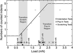
Nanoindentation and nanoscratching of an indium phosphide (InP) semiconductor surface was investigated via contact mechanics. Plastic deformation in InP is known to be caused by the nucleation, propagation, and multiplication of dislocations. Using selective electrochemical dissolution, which reveals dislocations at the semiconductor surface, the load needed to create the first dislocations in indentation and scratching can be determined. The experimental results showed that the load threshold to generate the first dislocations is twice lower in scratching compared to indentation. By modeling the elastic stress fields using contact mechanics based on Hertz’s theory, the results during scratching can be related to the friction between the surface and the tip. Moreover, Hertz’s model suggests that dislocations nucleate firstly at the surface and then propagate inside the bulk. The dislocation nucleation process explains the pop-in event which is characterized by a sudden extension of the indenter inside the surface during loading.

Type
Articles
Copyright
Copyright © Materials Research Society 2011

Access options

Get access to the full version of this content by using one of the access options below. (Log in options will check for institutional or personal access. Content may require purchase if you do not have access.)

References

REFERENCES

1.Oliver, W.C. and Pharr, G.M.: An improved technique for determining hardness and elastic modulus using load and displacement sensing indentation experiments. J. Mater. Res. 7, 1564 (1992).CrossRefGoogle Scholar
2.Ge, D., Domnich, V., and Gogotsi, Y.: High-resolution transmission-electron-microscopy study of metastable silicon phases produced by nanoindentation. J. Appl. Phys. 93, 2418 (2003).CrossRefGoogle Scholar
3.Gassilloud, R., Ballif, C., Gasser, P., Bürki, G., and Michler, J.: Deformation mechanisms of silicon during nanoscratching. Phys. Status Solidi A 202, 2858 (2005).CrossRefGoogle Scholar
4.Demarecaux, P., Chicot, D., and Lesage, J.: Interface indentation test for the determination of adhesive properties of thermal sprayed coatings. J. Mater. Sci. Lett. 15, 1377 (1996).CrossRefGoogle Scholar
5.Lawn, B.: Fracture of Brittle Solids 2nd ed. (Cambridge University Press, 1997).Google Scholar
6.Wasmer, K., Ballif, C., Gassilloud, R., Pouvreau, C., Rabe, R., Michler, J., Breguet, J.M., Solletti, J-M., Karimi, A., and Schulz, D.: Aspects of cleavage fracture of brittle semiconductors from the nanometre to the centimetre scale. Adv. Eng. Mater. 7, 309 (2005).CrossRefGoogle Scholar
7.Johnson, K.L.: Contact Mechanics (Cambridge University Press, Cambridge, 1985).CrossRefGoogle Scholar
8.Hill, R.: The Mathematical Theory of Plasticity (Clarendon Press, Oxford, 1950).Google Scholar
9.Leipner, H.S., Lorenz, D., Zeckzer, A., Lei, H., and Grau, P.: Nanoindentation pop-in effect in semiconductors. Physica B 308-310, 446 (2001).CrossRefGoogle Scholar
10.Bradby, J.E., Williams, J.S., and Wong-Leung, J.: Mechanical deformation of InP and GaAs by spherical indentation. Appl. Phys. Lett. 78, 3235 (2001).CrossRefGoogle Scholar
11.Bradby, J.E., Williams, J.S., and Swain, M.V.: Pop-in events induced by spherical indentation in compound semiconductors. J. Mater. Res. 19, 380 (2004).CrossRefGoogle Scholar
12.Bradby, J.E., Williams, J.S., Wong-Leung, J., Kucheyev, S.O., Swain, M.V., and Munroe, P.: Spherical indentation of compound semiconductors. Philos. Mag. A 82, 1931 (2002).CrossRefGoogle Scholar
13.Page, T.F., Oliver, C.O., and McHargue, C.J.: The deformation behavior of ceramic crystals subjected to very low load (nano)indentations. J. Mater. Res. 7, 450 (1992).CrossRefGoogle Scholar
14.Patriarche, G. and Le Bourhis, E.: Low-load deformation of InP under contact loading; comparison with GaAs. Philos. Mag. A 82, 1953 (2002).CrossRefGoogle Scholar
15.Almeida, C.M., Prioli, R., and Ponce, F.A.: Effect of native oxide mechanical deformation on InP nanoindentation. J. Appl. Phys. 104, 11509 (2008).CrossRefGoogle Scholar
16.Mann, A.B. and Pethica, J.B.: The role of atomic size asperities in the mechanical deformation of nanocontacts. Appl. Phys. Lett. 69, 907 (1996).CrossRefGoogle Scholar
17.Mann, A.B. and Pethica, J.B.: The effect of tip momentum on the contact stiffness and yielding during nanoindentation testing. Philos. Mag. A 79, 577 (1999).CrossRefGoogle Scholar
18.Huang, L-Y., Lu, J., and Xu, K-W.: The nano-scratch behaviour of different diamond-like carbon film-substrate. J. Phys. D: Appl. Phys. 37, 2135 (2004).CrossRefGoogle Scholar
19.Bhushan, B.: Handbook of Micro/Nano Tribology 2nd ed. (CRC Press, New York, 1999).Google Scholar
20.Ponce, F.A., Wei, Q.Y., Wu, Z.H., Fonseca-Filho, H.D., Almeida, C.M., Prioli, R., and Cherns, D.: Nanoscale dislocation patterning by scratching in an atomic force microscope. J. Appl. Phys. 106, 076106 (2009).CrossRefGoogle Scholar
21.Galdas, P.G., Prioli, R., Almeida, C.M., Huang, J.Y., and Ponce, F.A.: Plastic hardening in cubic semiconductors by nanoscratching. J. Appl. Phys. 109, 013502 (2011).Google Scholar
22.Wasmer, K., Parlinska-Wojtan, M., Gassilloud, R., Pouvreau, C., Tharian, J., and Michler, J.: Plastic deformation modes of gallium-arsenide in nanoindentation and nanoscratching. Appl. Phys. Lett. 90, 031902 (2007).CrossRefGoogle Scholar
23.Parlinska-Wojtan, M., Wasmer, K., Tharian, J., and Michler, J.: Microstructural comparison of material damage in GaAs caused by Berkovich and wedge nanoindentation and nanoscratching. Scr. Mater. 59, 364 (2008).CrossRefGoogle Scholar
24.Domnich, V. and Gogotsi, Y.: Phase transformation in silicon under contact loading. Rev. Adv. Mater. Sci. 3, 1 (2002).Google Scholar
25.Gogotsi, Y., Zhou, G., Ku, S-S., and Cetinkunt, S.: Raman microspectroscopy analysis of pressure-induced metallization in scratching of silicon. Semicond. Sci. Technol. 16, 345 (2001).CrossRefGoogle Scholar
26.Wasmer, K., Ballif, C., Pouvreau, C., Schulz, D., and Michler, J.: Dicing of gallium-arsenide high performance laser diodes for industrial applications: Part I: Scratching operation. J. Mater. Process. Technol. 198, 114 (2008).CrossRefGoogle Scholar
27.Wasmer, K., Ballif, C., Pouvreau, C., Schulz, D., and Michler, J.: Dicing of gallium-arsenide high performance laser diodes for industrial applications: Part II: Cleavage operation. J. Mater. Process. Technol. 198, 105 (2008).CrossRefGoogle Scholar
28.Michler, J., Gassilloud, R., Gasser, P., Santinacci, L., and Schmuki, P.: Defect-free AFM-scratching at the Si/SiO2-interface used for selective electrodeposition of nanowires. Electrochem. Solid-State Lett. 7, 41 (2004).CrossRefGoogle Scholar
29.Gassilloud, R., Michler, J., Ballif, C., Gasser, P., and Schmuki, P.: Selective etching of n-InP(100) triggered at surface dislocations induced by nanoscratching. Electrochim. Acta 51, 2182 (2005).CrossRefGoogle Scholar
30.Hanson, M.T.: The elastic field of spherical Hertzian contact including sliding friction for transverse isotropy. J. Tribol. 114, 606 (1992).CrossRefGoogle Scholar
31.Hanson, M.T. and Johnson, T.: The elastic field for spherical Hertzian contact of isotropic bodies revisited: Some alternative expression. J. Tribol. 115, 327 (1992).CrossRefGoogle Scholar
32.Le Bourhis, E. and Patriarche, G.: Plastic deformation of III-V semiconductors under concentrated load. Prog. Cryst. Growth Charact. Mater. 47, 1 (2003).CrossRefGoogle Scholar
33.Fischer-Cripp, A.C.: Nanoindentation (Ed. Mech Eng Series, Springer, New York, 2004).CrossRefGoogle Scholar
34.Nicholz, D.N., Rimai, D.S., and Sladek, R.J.: Elastic anharmonicity of InP: Its relationship to the high pressure transition. Solid State Commun. 36, 667 (1980).CrossRefGoogle Scholar
35.Adachi, S.: Properties of Group-IV, III-V, and II-VI Semiconductors (Wiley Series, Chichester, England, 2005).CrossRefGoogle Scholar
36.Le Bouhris, E.: In-depth structure of rosette arms in indium phosphide. J. Mater. Sci. Lett. 19, 167 (2000).CrossRefGoogle Scholar
37.Hess, P.: Laser diagnostic of mechanical and elastic properties of silicon and carbon films. Appl. Surf. Sci. 106, 429 (1996).CrossRefGoogle Scholar
38.Simmons, G. and Wang, H.: Single Crystal Elastic Constants and Calculated Aggregate Properties: A Handbook (MIT Press, Cambridge, Mass., 1971).Google Scholar
39.Yan, J., Tamaki, J., Zhao, H., and Kuriyagawa, T.: Surface and subsurface damages in nanoindentation tests of compound semiconductor InP. J. Micromech. Microeng. 18, 105018 (2008).CrossRefGoogle Scholar
40.Bhushan, B. and Li, X.: Micromechanical and tribological characterization of doped single-crystal silicon and polysilicon films for microelectromechanical systems devices. J. Mater. Res. 12(1), 54 (1997).CrossRefGoogle Scholar
41.Saxena, A.: Nonlinear Fracture Mechanics for Engineers, 1st ed. (CRC Press, New York, 1998).Google Scholar
42.Briscoe, B.J., Pelillo, E., Ragazzi, F., and Sinha, S.K.: Scratch deformation of methanol plasticized poly(methylmethacrylate) surfaces. Polymer 39, 2161 (1998).CrossRefGoogle Scholar
43.Dasari, A., Duncan, S.J., and Misra, R.D.K.: Micro- and nano-scale deformation processes during scratch damage in high density polyethylene. Mater. Sci. Technol. 19, 239 (2003).CrossRefGoogle Scholar
44.Bucaille, J.L., Felder, E., and Hochstetter, G.: Mechanical analysis of the scratch test on elastic and perfectly plastic materials with the three-dimensional finite element modeling. Wear 249, 422 (2001).CrossRefGoogle Scholar
45.Johnson, K.L.: The correlation of indentation experiments. J. Mech. Phys. Solids 18, 115 (1970).CrossRefGoogle Scholar
46.Madelung, O., Rössler, U., and Schulz, M.: Springer Materials—The Landolt-Börnstein Database DOI: 10.1007/10832182_298.CrossRefGoogle Scholar
47.Tabor, D.: The Hardness of Metals (Clarendon, Oxford 1951).Google Scholar
48.Hirth, J.P. and Lothe, J.: Theory of Dislocations 2nd ed. (John Wiley and Sons, 1982).Google Scholar
49.Azzaz, M., Michel, J-P., and George, A.: Plastic deformation, extended stacking faults and deformation twinning in single crystalline indium phosphide 2. S doped InP. Philos. Mag. A 73, 601 (1996).CrossRefGoogle Scholar
50.Le Bourhis, E., Patriarche, G., Riviere, J. P., and Zozime, A.: Material flow at the surface of indented indium phosphide. Phys. Status Solidi A 161, 415 (1997).3.0.CO;2-0>CrossRefGoogle Scholar
51.Le Bourhis, E. and Patriarche, G.: Deformation induced by Vickers indentor in InP at room temperature. Eur. Phys. J. Appl. Phys. 12, 31 (2000).CrossRefGoogle Scholar
52.Fisher-Cripps, A.C.: Introduction to Contact Mechanics (Springer, New York, 2000).Google Scholar
53.Ahn, Y., Farris, T.N., and Chandrasekar, S.: Sliding microindentation fracture of brittle materials: Role of elastic stress fields. Mech. Mater. 29, 143 (1998).CrossRefGoogle Scholar
54.Vanderschaeve, G.: Mechanical twinning in semiconductors. Solid State Phenom. 59-60, 145 (1998).CrossRefGoogle Scholar
55.Levade, C. and Vanderschaeve, G.: Rosette microstructure in indented (001) GaAs single crystals and the alpha/beta asymmetry. Phys. Status Solidi A 171, 83 (1999).3.0.CO;2-C>CrossRefGoogle Scholar
56.Dowling, N.E.: Mechanical Behavior of Materials (Prentice-Hall International, London, 1993).Google Scholar
57.Kamat, S.V. and Hirth, J.P.: Dislocation injection in strained multilayer strutures. J. Appl. Phys. 67, 6844 (1990).CrossRefGoogle Scholar
58.Alexander, H. and Haasen, P.: Dislocations and plastic flow in the diamond structure. Solid State Phys. 22, 27 (1968).CrossRefGoogle Scholar