Hostname: page-component-78c5997874-fbnjt Total loading time: 0 Render date: 2024-11-10T11:45:48.329Z Has data issue: false hasContentIssue false

Assessing atomically thin delta-doping of silicon using mid-infrared ellipsometry

Published online by Cambridge University Press:  23 June 2020

Aaron M. Katzenmeyer
Affiliation:
Sandia National Laboratories, Albuquerque, New Mexico, 87123, USA
Ting S. Luk
Affiliation:
Sandia National Laboratories, Albuquerque, New Mexico, 87123, USA
Ezra Bussmann
Affiliation:
Sandia National Laboratories, Albuquerque, New Mexico, 87123, USA
Steve Young
Affiliation:
Sandia National Laboratories, Albuquerque, New Mexico, 87123, USA
Evan M. Anderson
Affiliation:
Sandia National Laboratories, Albuquerque, New Mexico, 87123, USA
Michael T. Marshall
Affiliation:
Sandia National Laboratories, Albuquerque, New Mexico, 87123, USA
James A. Ohlhausen
Affiliation:
Sandia National Laboratories, Albuquerque, New Mexico, 87123, USA
Paul Kotula
Affiliation:
Sandia National Laboratories, Albuquerque, New Mexico, 87123, USA
Ping Lu
Affiliation:
Sandia National Laboratories, Albuquerque, New Mexico, 87123, USA
DeAnna M. Campbell
Affiliation:
Sandia National Laboratories, Albuquerque, New Mexico, 87123, USA
Tzu-Ming Lu
Affiliation:
Sandia National Laboratories, Albuquerque, New Mexico, 87123, USA
Peter Q. Liu
Affiliation:
Department of Electrical Engineering, The State University of New York at Buffalo, Buffalo, New York14260, USA
Daniel R. Ward
Affiliation:
Sandia National Laboratories, Albuquerque, New Mexico, 87123, USA
Shashank Misra*
Affiliation:
Sandia National Laboratories, Albuquerque, New Mexico, 87123, USA
*
a)Address all correspondence to this author. e-mail: smisra@sandia.gov
Get access

Abstract

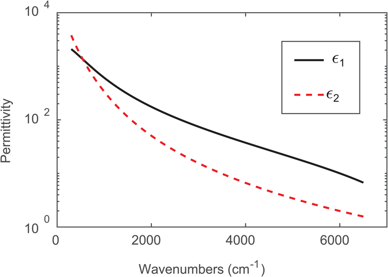
Hydrogen lithography has been used to template phosphine-based surface chemistry to fabricate atomic-scale devices, a process we abbreviate as atomic precision advanced manufacturing (APAM). Here, we use mid-infrared variable angle spectroscopic ellipsometry (IR-VASE) to characterize single-nanometer thickness phosphorus dopant layers (δ-layers) in silicon made using APAM compatible processes. A large Drude response is directly attributable to the δ-layer and can be used for nondestructive monitoring of the condition of the APAM layer when integrating additional processing steps. The carrier density and mobility extracted from our room temperature IR-VASE measurements are consistent with cryogenic magneto-transport measurements, showing that APAM δ-layers function at room temperature. Finally, the permittivity extracted from these measurements shows that the doping in the APAM δ-layers is so large that their low-frequency in-plane response is reminiscent of a silicide. However, there is no indication of a plasma resonance, likely due to reduced dimensionality and/or low scattering lifetime.

Type
Article
Copyright
Copyright © Materials Research Society 2020

Access options

Get access to the full version of this content by using one of the access options below. (Log in options will check for institutional or personal access. Content may require purchase if you do not have access.)

References

Ward, D.R., Schmucker, S.W., Anderson, E.M., Bussmann, E., Tracy, L.A., Lu, T.-M., Maurer, L.N., Baczewski, A., Campbell, D.M., Marshall, M.T., and Misra, S.: Atomic precision advanced manufacturing for digital electronics. Electron. Device Fail. Anal. Mag. 22, 410 (2020).Google Scholar
Zwanenburg, F.A., Dzurak, A.S., Morello, A., Simmons, M.Y., Hollenberg, L.C., Klimeck, G., Rogge, S., Coppersmith, S.N., and Eriksson, M.A.: Silicon quantum electronics. Rev. Mod. Phys. 85, 961 (2013).CrossRefGoogle Scholar
Sipahigil, A., Evans, R.E., Sukachev, D.D., Burek, M.J., Borregaard, J., Bhaskar, M.K., Nguyen, C.T., Pacheco, J.L., Atikian, H.A., and Meuwly, C.: An integrated diamond nanophotonics platform for quantum-optical networks. Science 354, 847850 (2016).CrossRefGoogle ScholarPubMed
Ward, D.R., Marshall, M.T., Campbell, D., Lu, T.-M., Koepke, J.C., Scrymgeour, D.A., Bussmann, E., and Misra, S.: All-optical lithography process for contacting nanometer precision donor devices. Appl. Phys. Lett. 111, 193101 (2017).CrossRefGoogle Scholar
Goh, K., Augarten, Y., Oberbeck, L., and Simmons, M.: Enhancing electron transport in Si: P delta-doped devices by rapid thermal anneal. Appl. Phys. Lett. 93, 142105 (2008).CrossRefGoogle Scholar
Bass, S.: Silicon and germanium doping of epitaxial gallium arsenide grown by the trimethylgallium-arsine method. J. Crystallogr. Growth 47, 613618 (1979).CrossRefGoogle Scholar
Zeindl, H., Wegehaupt, T., Eisele, I., Oppolzer, H., Reisinger, H., Tempel, G., and Koch, F.: Growth and characterization of a delta-function doping layer in Si. Appl. Phys. Lett. 50, 11641166 (1987).CrossRefGoogle Scholar
Gossmann, H.-J. and Schubert, E.: Delta doping in silicon. Crit. Rev. Solid State Mater. Sci. 18, 167 (1993).CrossRefGoogle Scholar
Oberbeck, L., Reusch, T.C., Hallam, T., Schofield, S.R., Curson, N.J., and Simmons, M.Y.: Imaging of buried phosphorus nanostructures in silicon using scanning tunneling microscopy. Appl. Phys. Lett. 104, 253102 (2014).CrossRefGoogle Scholar
Scrymgeour, D., Baca, A., Fishgrab, K., Simonson, R., Marshall, M., Bussmann, E., Nakakura, C., Anderson, M., and Misra, S.: Determining the resolution of scanning microwave impedance microscopy using atomic-precision buried donor structures. Appl. Surf. Sci. 423, 10971102 (2017).CrossRefGoogle Scholar
Gramse, G., Kölker, A., Lim, T., Stock, T.J., Solanki, H., Schofield, S.R., Brinciotti, E., Aeppli, G., Kienberger, F., and Curson, N.J.: Nondestructive imaging of atomically thin nanostructures buried in silicon. Sci. Adv. 3, e1602586 (2017).CrossRefGoogle ScholarPubMed
Bussmann, E., Rudolph, M., Subramania, G., Misra, S., Carr, S., Langlois, E., Dominguez, J., Pluym, T., Lilly, M., and Carroll, M.: Scanning capacitance microscopy registration of buried atomic-precision donor devices. Nanotechnology 26, 085701 (2015).CrossRefGoogle ScholarPubMed
Schmucker, S.W., Namboodiri, P.N., Kashid, R., Wang, X., Hu, B., Wyrick, J.E., Myers, A.F., Schumacher, J.D., Silver, R.M., and Stewart, M. Jr: Low-resistance, high-yield electrical contacts to atom scale Si: P devices using palladium silicide. Phys. Rev. Appl. 11, 034071 (2019).CrossRefGoogle ScholarPubMed
Miwa, J.A., Hofmann, P., Simmons, M.Y., and Wells, J.W.: Direct measurement of the band structure of a buried two-dimensional electron gas. Phys. Rev. Lett. 110, 136801 (2013).CrossRefGoogle ScholarPubMed
Boher, P., Bucchia, M., Guillotin, C., and Defranoux, C.: Infrared spectroscopic ellipsometry applied to the characterization of nano-structures of silicon IC manufacturing. Thin Solid Films 450, 173177 (2004).CrossRefGoogle Scholar
Woollam, J.A. and Snyder, P.G.: Fundamentals and applications of variable angle spectroscopic ellipsometry. Mater. Sci. Eng. B 5, 279283 (1990).CrossRefGoogle Scholar
Woollam, J.A., Johs, B.D., Herzinger, C.M., Hilfiker, J.N., Synowicki, R.A., and Bungay, C.L.: Overview of variable-angle spectroscopic ellipsometry (VASE): I. Basic theory and typical applications. In Optical Metrology: A Critical Review, Proc. SPIE 10294, 1029402 (1999). doi:10.1117/12.351660.CrossRefGoogle Scholar
Dorvel, B., Reddy, B. Jr, Block, I., Mathias, P., Clare, S.E., Cunningham, B., Bergstrom, D.E., and Bashir, R.: Vapor-phase deposition of monofunctional alkoxysilanes for sub-nanometer-level biointerfacing on silicon oxide surfaces. Adv. Funct. Mater. 20, 8795 (2010).CrossRefGoogle Scholar
Nelson, F., Kamineni, V., Zhang, T., Comfort, E., Lee, J., and Diebold, A.: Optical properties of large-area polycrystalline chemical vapor deposited graphene by spectroscopic ellipsometry. Appl. Phys. Lett. 97, 253110 (2010).CrossRefGoogle Scholar
Tiwald, T.E., Thompson, D.W., Woollam, J.A., Paulson, W., and Hance, R.: Application of IR variable angle spectroscopic ellipsometry to the determination of free carrier concentration depth profiles. Thin Solid Films 313, 661666 (1998).CrossRefGoogle Scholar
Pidgeon, C.: Free carrier optical properties. Handb. Semiconduct. 2, 223328 (1980).Google Scholar
Ginn, J.C., Jarecki, R.L. Jr, Shaner, E.A., and Davids, P.S.: Infrared plasmons on heavily-doped silicon. J. Appl. Phys. 110, 043110 (2011).CrossRefGoogle Scholar
Katzenmeyer, A. M., Dmitrovic, S., Baczewski, A. D., Bussmann, E., Lu, T.-M., Anderson, E., Schmucker, S., Ivie, J. A., Campbell, D. M., Ward, D. R., Wang, G. T., and Misra, S.: Photothermal alternative to device fabrication using atomic precision advanced manufacturing techniques. Proc. SPIE 11324, 113240Z (2020). doi: 10.1117/12.2551455.CrossRefGoogle Scholar
Hagmann, J.A., Wang, X., Namboodiri, P., Wyrick, J., Murray, R., Stewart, M. Jr, Silver, R.M., and Richter, C.A.: High resolution thickness measurements of ultrathin Si: P monolayers using weak localization. Appl. Phys. Lett. 112, 043102 (2018).CrossRefGoogle Scholar
Polley, C.M., Clarke, W.R., Miwa, J.A., Scappucci, G., Wells, J.W., Jaeger, D.L., Bischof, M.R., Reidy, R.F., Gorman, B.P., and Simmons, M.: Exploring the limits of n-type ultra-shallow junction formation. ACS Nano 7, 54995505 (2013).CrossRefGoogle ScholarPubMed
Matmon, G., Ginossar, E., Villis, B.J., Kölker, A., Lim, T., Solanki, H., Schofield, S.R., Curson, N.J., Li, J., and Murdin, B.N.: Two-to three-dimensional crossover in a dense electron liquid in silicon. Phys. Rev. B 97, 155306 (2018).CrossRefGoogle Scholar
Hwang, E. and Sarma, S.D.: Electronic transport in two-dimensional Si: P δ-doped layers. Phys. Rev. B 87, 125411 (2013).CrossRefGoogle Scholar
Hilfiker, J.N., Stadermann, M., Sun, J., Tiwald, T., Hale, J.S., Miller, P.E., and Aracne-Ruddle, C.: Determining thickness and refractive index from free-standing ultra-thin polymer films with spectroscopic ellipsometry. Appl. Surf. Sci. 421, 508512 (2017).CrossRefGoogle Scholar
Cleary, J., Peale, R., Shelton, D., Boreman, G., Smith, C., Ishigami, M., Soref, R., Drehman, A., and Buchwald, W.: IR permittivities for silicides and doped silicon. J. Opt. Soc. Am. B 27, 730734 (2010).CrossRefGoogle Scholar
Shahzad, M., Medhi, G., Peale, R.E., Buchwald, W.R., Cleary, J.W., Soref, R., Boreman, G.D., and Edwards, O.: Infrared surface plasmons on heavily doped silicon. J. Appl. Phys. 110, 123105 (2011).CrossRefGoogle Scholar
Salman, J., Hafermann, M., Rensberg, J., Wan, C., Wambold, R., Gundlach, B.S., Ronning, C., and Kats, M.A.: Flat optical and plasmonic devices using area-selective ion-beam doping of silicon. Adv. Opt. Mater. 6, 1701027 (2018).CrossRefGoogle Scholar
Škereň, T., Pascher, N., Garnier, A., Reynaud, P., Rolland, E., Thuaire, A., Widmer, D., Jehl, X., and Fuhrer, A.: CMOS platform for atomic-scale device fabrication. Nanotechnology 29, 435302 (2018).CrossRefGoogle ScholarPubMed
Stern, F.: Polarizability of a two-dimensional electron gas. Phys. Rev. Lett. 18, 546 (1967).CrossRefGoogle Scholar
Davies, J.H.: The Physics of Low-dimensional Semiconductors: An Introduction (Cambridge University Press, Cambridge, UK, 1998), pp. 353356.Google Scholar
Hunderi, O. and Ryberg, R.: Amorphous gallium-a free electron metal. J. Phys. F: Metal. Phys. 4, 2096 (1974).CrossRefGoogle Scholar