Hostname: page-component-cd9895bd7-dk4vv Total loading time: 0 Render date: 2024-12-28T05:26:09.692Z Has data issue: false hasContentIssue false

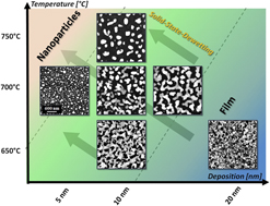
Fabrication and determination of growth regimes of various Pd NPs based on the control of deposition amount and temperature on c-plane GaN

Published online by Cambridge University Press:  17 July 2017
Mao Sui
Affiliation:
College of Electronics and Information, Kwangwoon University, Nowon-gu Seoul 01897, South Korea
Sundar Kunwar
Affiliation:
College of Electronics and Information, Kwangwoon University, Nowon-gu Seoul 01897, South Korea
Puran Pandey
Affiliation:
College of Electronics and Information, Kwangwoon University, Nowon-gu Seoul 01897, South Korea
Quanzhen Zhang
Affiliation:
College of Electronics and Information, Kwangwoon University, Nowon-gu Seoul 01897, South Korea
Ming-Yu Li
Affiliation:
College of Electronics and Information, Kwangwoon University, Nowon-gu Seoul 01897, South Korea
Jihoon Lee*
Affiliation:
College of Electronics and Information, Kwangwoon University, Nowon-gu Seoul 01897, South Korea; and Institute of Nanoscale Science and Engineering, University of Arkansas, Fayetteville, Arkansas 72701, USA
*
a) Address all correspondence to this author. e-mail: jihoonleenano@gmail.com
Get access

Abstract

Palladium (Pd) nanostructures have been actively adapted for various applications and their properties and applicability closely depend on their shape, size, and density. In this paper, the evolution of self-assembled Pd nanostructures on the hexagonal c-plane GaN is presented by the systematical control of Pd deposition amount (DA) at distinctive temperatures. Pd nanostructures of various configurations, sizes, and densities are demonstrated based on the solid-state dewetting of Pd thin films and a clear distinction in the growth regimes is observed. Three growth regimes are clearly observed depending on the variation of DA, i.e., (i) the agglomeration of Pd nanoparticles, (ii) the coalescence of wiggly Pd nanostructures, and finally (iii) the growth of nanovoids and layers. Owing to the temperature-dependent dewetting process, the growth regimes are markedly shifted, resulting in the distinctive Pd nanostructures within the identical DA range. The results are discussed in conjunction with the surface diffusion, Volmer–Weber and coalescence growth model, and surface/interface energy minimization mechanism. In addition, the evolution of optical properties, emission band, and lattice properties are probed by reflectance, photoluminescence, and Raman spectroscopy, which exhibit varying spectral intensity and peak positions according to the surface morphology of Pd nanostructures.

Type
Articles
Copyright
Copyright © Materials Research Society 2017 

Access options

Get access to the full version of this content by using one of the access options below. (Log in options will check for institutional or personal access. Content may require purchase if you do not have access.)

Footnotes

Contributing Editor: Jürgen Eckert

References

REFERENCES

Wolfe, J.P., Singer, R.A., Yang, B.H., and Buchwald, S.L.: Highly active palladium catalysts for Suzuki coupling reactions. J. Am. Chem. Soc. 121, 9550 (1999).Google Scholar
Reetz, M.T. and Westermann, E.: Phosphane-free palladium-catalyzed coupling reactions: The decisive role of Pd nanoparticles. Angew. Chem., Int. Ed. 39, 165 (2000).Google Scholar
Beletskaya, I.P. and Cheprakov, A.V.: The Heck reaction as a sharpening stone of palladium catalysis. Chem. Rev. 100, 3009 (2000).Google Scholar
Tian, N., Zhou, Z.Y., Yu, N.F., Wang, L.Y., and Sun, S.G.: Direct electrodeposition of tetrahexahedral Pd nanocrystals with high-index facets and high catalytic activity for ethanol electro-oxidation. J. Am. Chem. Soc. 132, 7580 (2010).Google Scholar
Mori, K., Hara, T., Mizugaki, T., Ebitani, K., and Kaneda, K.: Hydroxyapatite-supported palladium nanoclusters: A highly active heterogeneous catalyst for selective oxidation of alcohols by use of molecular oxygen. J. Am. Chem. Soc. 126, 10657 (2004).CrossRefGoogle ScholarPubMed
Sales, E.A., de Jesus Mendes, M., and Bozon-Verduraz, F.: Liquid-phase selective hydrogenation of hexa-1,5-diene and hexa-1,3-diene on palladium catalysts. Effect of tin and silver addition. J. Catal. 195, 96 (2000).CrossRefGoogle Scholar
Vilé, G., Albani, D., Nachtegaal, M., Chen, Z., Dontsova, D., Antonietti, M., Lopez, N., and Perez-Ramirez, J.: A stable single-site palladium catalyst for hydrogenations. Angew. Chem., Int. Ed. 54, 11265 (2015).CrossRefGoogle ScholarPubMed
Cheon, Y.E. and Suh, M.P.: Enhanced hydrogen storage by palladium nanoparticles fabricated in a redox-active metal-organic framework. Angew. Chem. 121, 2943 (2009).Google Scholar
Pundt, A., Sachs, C., Winter, M., Reetz, M.T., Fritsch, D., and Kirchheim, R.: Hydrogen sorption in elastically soft stabilized Pd-clusters. J. Alloys Compd. 293, 480483 (1999).Google Scholar
Shan, X., Payer, J.H., Wainright, J.S., and Dudik, L.: A micro-fabricated hydrogen storage module with sub-atmospheric activation and durability in air exposure. J. Power Sources 196, 827 (2011).Google Scholar
Du, Y., Xue, Q., Zhang, Z., Xia, F., Li, J., and Han, Z.: Hydrogen gas sensing properties of Pd/aC:Pd/SiO2/Si structure at room temperature. Sens. Actuators, B 186, 796801 (2013).Google Scholar
Lim, S.H., Radha, B., Chan, J.Y., Saifullah, M.S., Kulkarni, G.U., and Ho, G.W.: Flexible palladium-based H2 sensor with fast response and low leakage detection by nanoimprint lithography. ACS Appl. Mater. Interfaces 5, 7274 (2013).CrossRefGoogle ScholarPubMed
Šlouf, M., Pavlova, E., Bhardwaj, M., Pleštil, J., Onderková, H., Philimonenko, A.A., and Hozák, P.: Preparation of stable Pd nanoparticles with tunable size for multiple immunolabeling in biomedicine. Mater. Lett. 65, 1197 (2011).Google Scholar
Gavia, D.J. and Shon, Y.S.: Controlling surface ligand density and core size of alkanethiolate-capped Pd nanoparticles and their effects on catalysis. Langmuir 28, 14502 (2012).Google Scholar
Le Ru, E. and Etchegoin, P.: Principles of Surface-Enhanced Raman Spectroscopy: And Related Plasmonic Effects; Introduction to Plasmons and Plasmonics (Elsevier, Amsterdam, the Netherlands 2008); ch. 3, p. 128.Google Scholar
Langhammer, C., Yuan, Z., Zorić, I., and Kasemo, B.: Plasmonic properties of supported Pt and Pd nanostructures. Nano Lett. 6, 833 (2006).CrossRefGoogle ScholarPubMed
Cui, L., Wang, A., Wu, D.Y., Ren, B., and Tian, Z.Q.: Shaping and shelling Pt and Pd nanoparticles for ultraviolet laser excited surface-enhanced Raman scattering. J. Phys. Chem. C 112, 17618 (2008).Google Scholar
Cui, L., Mahajan, S., Cole, R.M., Soares, B., Bartlett, P.N., Baumberg, J.J., Hayward, I.P., Ren, B., Russell, A.E., and Tian, Z.Q.: UV SERS at well-ordered Pd sphere segment void (SSV) nanostructures. Phys. Chem. Chem. Phys. 11, 1023 (2009).CrossRefGoogle ScholarPubMed
Thompson, C.V.: Solid-state dewetting of thin films. Annu. Rev. Mater. Res. 42, 399 (2012).Google Scholar
Zhao, X., Lee, U.J., and Lee, K.H.: Dewetting behavior of Au films on porous substrates. Thin Solid Films 519, 706 (2010).Google Scholar
Wang, D. and Schaaf, P.: Solid state dewetting for fabrication of metallic nanoparticles and influences of nanostructured substrates and dealloying. Phys. Status Solidi A 210, 1544 (2013).Google Scholar
Ruffino, F. and Grimaldi, M.G.: Dewetting of template-confined Au films on SiC surface: From patterned films to patterned arrays of nanoparticles. Vacuum 99, 28 (2014).Google Scholar
Danielson, D.T., Sparacin, D.K., Michel, J., and Kimerling, L.C.: Surface-energy-driven dewetting theory of silicon-on-insulator agglomeration. J. Appl. Phys. 100, 083507 (2006).Google Scholar
Ruffino, F., Canino, A., Grimaldi, M.G., Giannazzo, F., Bongiorno, C., Roccaforte, F., and Raineri, V.: Self-organization of gold nanoclusters on hexagonal SiC and SiO2 surfaces. J. Appl. Phys. 101, 064306 (2007).Google Scholar
Volmer, M. and Weber, A.: Nucleus formation in supersaturated systems. Z. Phys. Chem. 119, 277 (1926).Google Scholar
Venables, J.A., Spiller, G.D.T., and Hanbucken, M.: Nucleation and growth of thin films. Rep. Prog. Phys. 47, 399 (1984).Google Scholar
Sui, M., Li, M.Y., Kim, E.S., and Lee, J.H.: Mini droplets to super droplets: Evolution of self-assembled Au droplets on GaAs (111) B and (110). J. Appl. Crystallogr. 47, 505 (2014).Google Scholar
Li, C.R., Lu, N.P., Mei, J., Dong, W.J., Zheng, Y.Y., Gao, L., Tsukamoto, K., and Cao, Z.X.: Polyhedral to nearly spherical morphology transformation of silver microcrystals grown from vapor phase. J. Cryst. Growth 314, 324 (2011).Google Scholar
Ruffino, F. and Grimaldi, M.G.: Atomic force microscopy study of the growth mechanisms of nanostructured sputtered Au film on Si(111): Evolution with film thickness and annealing time. J. Appl. Phys. 107, 104321 (2010).Google Scholar
Ruffino, F. and Grimaldi, M.G.: Island-to-percolation transition during the room-temperature growth of sputtered nanoscale Pd films on hexagonal SiC. J. Appl. Phys. 107, 074301 (2010).CrossRefGoogle Scholar
Sui, M., Pandey, P., Li, M.Y., Zhang, Q., Kunwar, S., and Lee, J.H.: Tuning the configuration of Au nanostructures: From vermiform-like, rod-like, triangular, hexagonal, to polyhedral nanostructures on c-plane GaN. J. Mater. Sci. 52, 391 (2017).Google Scholar
Pandey, P., Sui, M., Zhang, Q., Li, M.Y., Kunwar, S., and Lee, J.H.: Systematic control of the size, density and configuration of Pt nanostructures on sapphire (0001) by the variation of deposition amount and dwelling time. Appl. Surf. Sci. 368, 198 (2016).Google Scholar
Li, M.Y., Sui, M., Pandey, P., Zhang, Q., Kim, E.S., and Lee, J.H.: Systematic control of self-assembled Au nanoparticles and nanostructures through the variation of deposition amount, annealing duration, and temperature on Si(111). Nanoscale Res. Lett. 10, 380 (2015).CrossRefGoogle ScholarPubMed
Lee, D., Li, M.Y., Sui, M., Zhang, Q., Pandey, P., Kim, E.S., and Lee, J.H.: Observation of shape, configuration, and density of Au nanoparticles on various GaAs surfaces via deposition amount, annealing temperature, and dwelling time. Nanoscale Res. Lett. 10, 240 (2015).Google Scholar
Lian, C.X., Li, X.Y., and Liu, J.: Optical anisotropy of wurtzite GaN on sapphire characterized by spectroscopic ellipsometry. Semicond. Sci. Technol. 19, 417 (2003).CrossRefGoogle Scholar
Fabian, M., Lewis, E., Newe, T., and Lochmann, S.: Optical fibre cavity for ring-down experiments with low coupling losses. Meas. Sci. Technol. 21, 094034 (2010).Google Scholar
Yannopapas, V.: Periodic arrays of film-coupled cubic nanoantennas as tunable plasmonic metasurfaces. Photonics 2, 270 (2015).Google Scholar
Leong, K.H., Chu, H.Y., Ibrahim, S., and Saravanan, P.: Palladium nanoparticles anchored to anatase TiO2 for enhanced surface plasmon resonance-stimulated, visible-light-driven photocatalytic activity. Beilstein J. Nanotechnol. 6, 428 (2015).Google Scholar
Mandal, M., Kundu, S., Ghosh, S.K., and Pal, T.: Micelle-mediated UV-photoactivation route for the evolution of Pd core–Au shell and Pd core–Ag shell bimetallics from photogenerated Pd nanoparticles. J. Photochem. Photobiol., A 167, 17 (2004).Google Scholar
Li, X. and Wang, Y.: Structure and photoluminescence properties of Ag-coated ZnO nano-needles. J. Alloys Compd. 509, 5765 (2011).Google Scholar
Liang, Y., Guo, N., Li, L., Li, R., Ji, G., and Gan, S.: Facile synthesis of Ag/ZnO micro-flowers and their improved ultraviolet and visible light photocatalytic activity. New J. Chem. 40, 1587 (2016).CrossRefGoogle Scholar
Zhang, L., Yu, J., Hao, X., Wu, Y., Dai, Y., Shao, Y., Zhang, H., and Tian, Y.: Influence of stress in GaN crystals grown by HVPE on MOCVD-GaN/6H-SiC substrate. Sci. Rep. 4, 4179 (2014).CrossRefGoogle ScholarPubMed
Aumer, M.E., LeBoeuf, S.F., Bedair, S.M., Aumer, M.E., Smith, M., Lin, J.Y., and Jiang, H.X.: Effects of tensile and compressive strain on the luminescence properties of AlInGaN/InGaN quantum well structures. Appl. Phys. Lett. 77, 821 (2000).Google Scholar
Ishioka, K., Kato, K., Ohashi, N., Haneda, H., Kitajima, M., and Petek, H.: The effect of n-and p-type doping on coherent phonons in GaN. J. Phys. C: Solid State Phys. 25, 205404 (2013).Google Scholar
Eason, R.: Pulsed laser deposition of thin films: Applications-led growth of functional materials. In Growth Kinetics During Pulsed Laser Deposition, Eason, R., ed. (John Wiley & Sons, USA, 2007); ch. 8, p. 178.Google Scholar
Supplementary material: File

Sui supplementary material

Sui supplementary material

Download Sui supplementary material(File)
File 11.5 MB