Hostname: page-component-78c5997874-s2hrs Total loading time: 0 Render date: 2024-11-10T11:16:26.207Z Has data issue: false hasContentIssue false

Palladium seeded GaAs nanowires

Published online by Cambridge University Press:  14 January 2016

Robert T. Hallberg*
Affiliation:
Solid State Physics, Lund University, 221 00 Lund, Sweden
Sebastian Lehmann
Affiliation:
Solid State Physics, Lund University, 221 00 Lund, Sweden
Maria E. Messing
Affiliation:
Solid State Physics, Lund University, 221 00 Lund, Sweden; and Synchrotron Radiation Research, Lund University, 211 00, Lund, Sweden
Kimberly A. Dick
Affiliation:
Solid State Physics, Lund University, 221 00 Lund, Sweden; and Centre for Analysis and Synthesis, Lund University, 221 00 Lund, Sweden
*
a) Address all correspondence to this author. e-mail: robert.hallberg@ftf.lth.se
Get access

Abstract

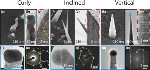
In this work, we present a detailed investigation of the growth of palladium-seeded GaAs nanowires. Nanowires grown on GaAs (111)B substrates consist of three different morphologies, denoted as curly (containing multiple kinks), inclined (relative to the substrate, such as 〈001〉), and vertical. We show that the relative yield of the different types is controllable by a combination of V/III ratio and temperature, where vertical and inclined nanowires are promoted by a high temperature and low V/III ratio. These growth conditions are expected to promote a higher Ga incorporation into the Pd particle, which is confirmed by energy dispersive x-ray analysis. We propose that the observed relationship between particle composition and nanowire morphology may be related to the particle phase, with liquid particles promoting straight nanowire growth. In addition, particles at the tips of nanowires are sometimes observed to be smaller than the initial particle size, suggesting that Pd has been lost during the growth process. Finally, we demonstrate the importance of initial particle size-control to interpret diameter changes after growth.

Type
Invited Feature Paper
Copyright
Copyright © Materials Research Society 2016 

Access options

Get access to the full version of this content by using one of the access options below. (Log in options will check for institutional or personal access. Content may require purchase if you do not have access.)

References

REFERENCES

Dick, K.A.: A review of nanowire growth promoted by alloys and non-alloying elements with emphasis on Au-assisted III–V nanowires. Prog. Cryst. Growth Charact. Mater. 54(3–4), 138173 (2008).CrossRefGoogle Scholar
Tavendale, A.J. and Pearton, S.J.: Deep level, quenched-in defects in silicon doped with gold, silver, iron, copper or nickel. J. Phys. C: Solid State Phys. 16(9), 16651673 (1983).Google Scholar
Hornstra, J.: Dislocations in the diamond lattice. J. Phys. Chem. Solids 5(1–2), 129141 (1958).Google Scholar
Schroer, M.D. and Petta, J.R.: Correlating the nanostructure and electronic properties of InAs nanowires. Nano Lett. 10(5), 16181622 (2010).CrossRefGoogle ScholarPubMed
Thelander, C., Caroff, P., Plissard, S., Dey, A.W., and Dick, K.A.: Effects of crystal phase mixing on the electrical properties of InAs nanowires. Nano Lett. 11(6), 24242429 (2011).Google Scholar
Xu, H., Wang, Y., Guo, Y., Liao, Z., and Gao, Q.: Defect-free <110> zinc-blende structured InAs nanowires catalyzed by palladium. Nano Lett. 12, 57445749 (2012).Google Scholar
Regolin, I., Khorenko, V., Prost, W., Tegude, F.J., Sudfeld, D., Kästner, J., Dumpich, G., Hitzbleck, K., and Wiggers, H.: GaAs whiskers grown by metal-organic vapor-phase epitaxy using Fe nanoparticles. J. Appl. Phys. 101(5), 15 (2007).CrossRefGoogle Scholar
Heun, S., Radha, B., Ercolani, D., Kulkarni, G.U., Rossi, F., Grillo, V., Salviati, G., Beltram, F., and Sorba, L.: Coexistence of vapor-liquid-solid and vapor-solid-solid growth modes in Pd-assisted InAs nanowires. Small 6(17), 19351941 (2010).Google Scholar
Heun, S., Radha, B., Ercolani, D., Kulkarni, G.U., Rossi, F., Grillo, V., Salviati, G., Beltram, F., and Sorba, L.: Pd-assisted growth of InAs nanowires. Cryst. Growth Des. 10(9), 41974202 (2010).Google Scholar
Hillerich, K., Ghidini, D.S., Dick, K.A., Deppert, K., and Johansson, J.: Cu particle seeded InP–InAs axial nanowire heterostructures. Phys. Status Solidi RRL 7(10), 850854 (2013).Google Scholar
Sun, R., Jacobsson, D., Chen, I-J., Nilsson, M., Thelander, C., Lehmann, S., and Dick, K.A.: Sn-seeded GaAs nanowires as self-assembled radial p-n junctions. Nano Lett. 15(6), 37573762 (2015).Google Scholar
Martelli, F., Rubini, S., Piccin, M., Bais, G., Jabeen, F., De Franceschi, S., Grillo, V., Carlino, E., D'Acapito, F., Boscherini, F., Cabrini, S., Lazzarino, M., Businaro, L., Romanato, F., and Franciosi, A.: Manganese-induced growth of GaAs nanowires. Nano Lett. 6(9), 21302134 (2006).Google Scholar
Jabeen, F., Piccin, M., Felisari, L., Grillo, V., Bais, G., Rubini, S., Martelli, F., D'Acapito, F., Rovezzi, M., and Boscherini, F.: Mn-induced growth of InAs nanowires. J. Vac. Sci. Technol., B 28(3), 478 (2010).CrossRefGoogle Scholar
Vogel, A.T., de Boor, J., Becker, M., Wittemann, J.V., Mensah, S.L., Werner, P., and Schmidt, V.: Ag-assisted CBE growth of ordered InSb nanowire arrays. Nanotechnology 22(1), 015605 (2011).Google Scholar
Fanfair, D.D. and Korgel, B.A.: Bismuth nanocrystal-seeded III-V semiconductor nanowire synthesis. Cryst. Growth Des. 5(5), 19711976 (2005).Google Scholar
Zhuang, H-Z., Li, B.L., Xue, C.S., Zhang, X., Zhang, S.Y., Wang, D-X., and Shen, J.B.: Growth of Nb-catalysed GaN nanowires. Microelectron. J. 39(12), 16291633 (2008).Google Scholar
Weng, X., Burke, R., and Redwing, J.: The nature of catalyst particles and growth mechanisms of GaN nanowires grown by Ni-assisted metal–organic chemical vapor deposition. Nanotechnology 20, 15 (2009).CrossRefGoogle ScholarPubMed
Li, H., Xue, C., Zhuyang, H., Chen, J., Yang, Z., Qin, L., Huang, Y., and Zhang, D.: Synthesis and characterization of GaN nanowires with Tantalum catalyst. Mater. Chem. Phys. 109(2–3), 249252 (2008).CrossRefGoogle Scholar
Chen, J., Xue, C., Zhuang, H., Qin, L., Li, H., and Yang, Z.: Synthesis of GaN nanowires by Tb catalysis. Appl. Surf. Sci. 254(15), 47164719 (2008).Google Scholar
Wagner, R.S. and Ellis, W.C.: Vapor-liquid-solid mechanism of single crystal growth. Appl. Phys. Lett. 4(5), 8990 (1964).Google Scholar
Persson, A.I., Larsson, M.W., Stenström, S., Ohlsson, B.J., Samuelson, L., and Wallenberg, L.R.: Solid-phase diffusion mechanism for GaAs nanowire growth. Nat. Mater. 3(10), 677681 (2004).CrossRefGoogle ScholarPubMed
Chou, Y.C., Wen, C.Y., Reuter, M.C., Su, D., Stach, E.A., and Ross, F.M.: Controlling the growth of Si/Ge nanowires and heterojunctions using silver-gold alloy catalysts. ACS Nano 6(7), 64076415 (2012).CrossRefGoogle ScholarPubMed
Ross, F.M., Wen, C-Y., Kodambaka, S., Wacaser, B.A., Reuter, M.C., and Stach, E.A.: The growth and characterization of Si and Ge nanowires grown from reactive metal catalysts. Philos. Mag. 90(20), 28072816 (2010).CrossRefGoogle Scholar
Kodambaka, S., Tersoff, J., Reuter, M.C., and Ross, F.M.: Germanium nanowire growth below the eutectic temperature. Science 316(5825), 729732 (2007).Google Scholar
Hofmann, S., Sharma, R., Wirth, C.T., Cervantes-Sodi, F., Ducati, C., Kasama, T., Dunin-Borkowski, R.E., Drucker, J., Bennett, P., and Robertson, J.: Ledge-flow-controlled catalyst interface dynamics during Si nanowire growth. Nat. Mater. 7(5), 372375 (2008).Google Scholar
Hillerich, K., Dick, K.A., Messing, M.E., Deppert, K., and Johansson, J.: Simultaneous growth mechanisms for Cu-seeded InP nanowires. Nano Res. 5(5), 297306 (2012).CrossRefGoogle Scholar
Meuller, B.O., Messing, M.E., Engberg, D.L.J., Jansson, A.M., Johansson, L.I.M., Norlén, S.M., Tureson, N., and Deppert, K.: Review of spark discharge generators for production of nanoparticle aerosols. Aerosol Sci. Technol. 46(11), 12561270 (2012).Google Scholar
Johansson, J., Dick, K.A., Caroff, P., Messing, M.E., Bolinsson, J., Deppert, K., and Samuelson, L.: Diameter dependence of the wurtzite-zinc blende transition in InAs nanowires. J. Phys. Chem. C 114(9), 38373842 (2010).CrossRefGoogle Scholar
Borg, B.M., Johansson, J., Storm, K., and Deppert, K.: Geometric model for metalorganic vapour phase epitaxy of dense nanowire arrays. J. Cryst. Growth 366, 1519 (2013).Google Scholar
Storm, K.: NanoDim Software. http://nanodim.kristian.storm.com (accessed December 03 2015).Google Scholar
Predel, B.: Ga-Pd (Gallium-Palladium). In Landolt-Börnstein – Group IV Physical Chemistry, Ga-Gd – Hf-Zr, Madelung, O., ed. (Springer-Verlag: Berlin, 1996); pp. 5759.Google Scholar
Thombare, S.V., Marshall, A.F., and McIntyre, P.C.: Size effects in vapor-solid-solid Ge nanowire growth with a Ni-based catalyst. J. Appl. Phys. 112(054325), 06 (2012).Google Scholar
Wen, C-Y., Tersoff, J., Reuter, M.C., Stach, E.A., and Ross, F.M.: Step-flow kinetics in nanowire growth. Phys. Rev. Lett. 105(19), 14 (2010).CrossRefGoogle ScholarPubMed
Xu, H., Guo, Y., Liao, Z., and Sun, W.: Catalyst size dependent growth of Pd-catalyzed one-dimensional InAs nanostructures. Appl. Phys. Lett. 102, 203108 (2013).Google Scholar
Schmidt, V.: Diameter-dependent growth direction of epitaxial silicon nanowires. Nano Lett. 5(5), 931935 (2005).CrossRefGoogle ScholarPubMed
Cai, R.G., Gong, Y., and Wang, B.: The size-dependent growth direction of ZnSe nanowires. Adv. Mater. 18, 109114 (2006).Google Scholar
Zhang, Z., Zheng, K., Lu, Z-Y., Chen, P-P., Lu, W., and Zou, J.: Catalyst orientation-induced growth of defect-free zinc-blende structured $\left\langle {00\bar 1} \right\rangle$ InAs nanowires. Nano Lett. 15, 876882 (2015).Google Scholar
Joyce, H.J., Gao, Q., Tan, H.H., Jagadish, C., Kim, Y., Zhang, X., Guo, Y., and Zou, J.: Twin-free uniform epitaxial GaAs nanowires grown by a two-temperature process. Nano Lett. 7(4), 921926 (2007).Google Scholar
Supplementary material: File

Hallberg supplementary material

Hallberg supplementary material 1

Download Hallberg supplementary material(File)
File 766.3 KB
Supplementary material: Image

Hallberg supplementary material

Hallberg supplementary material 2

Download Hallberg supplementary material(Image)
Image 1.8 MB
Supplementary material: Image

Hallberg supplementary material

Hallberg supplementary material 3

Download Hallberg supplementary material(Image)
Image 2.8 MB
Supplementary material: Image

Hallberg supplementary material

Hallberg supplementary material 4

Download Hallberg supplementary material(Image)
Image 2.5 MB
Supplementary material: Image

Hallberg supplementary material

Hallberg supplementary material 5

Download Hallberg supplementary material(Image)
Image 4.7 MB
Supplementary material: Image

Hallberg supplementary material

Hallberg supplementary material 6

Download Hallberg supplementary material(Image)
Image 6.3 MB
Supplementary material: Image

Hallberg supplementary material

Hallberg supplementary material 7

Download Hallberg supplementary material(Image)
Image 3.2 MB