Hostname: page-component-cd9895bd7-q99xh Total loading time: 0 Render date: 2024-12-28T07:49:37.409Z Has data issue: false hasContentIssue false

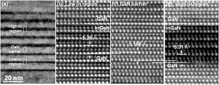
Quantitative compositional analysis of InxGa1−xN/GaN multiquantum wells in light-emitting diodes

Published online by Cambridge University Press:  06 July 2015
Youngji Cho
Affiliation:
Department of Measurement & Analysis, National Nanofab Center, Daejeon 305-806, Korea; and Department of Applied Science, Korea Maritime and Ocean University, Busan 606-791, Korea
Jung Sik Park
Affiliation:
Department of Measurement & Analysis, National Nanofab Center, Daejeon 305-806, Korea
Jun-Mo Yang*
Affiliation:
Department of Measurement & Analysis, National Nanofab Center, Daejeon 305-806, Korea
Kyung Jin Park
Affiliation:
Department of Measurement & Analysis, National Nanofab Center, Daejeon 305-806, Korea
Yun Chang Park
Affiliation:
Department of Measurement & Analysis, National Nanofab Center, Daejeon 305-806, Korea
Jiho Chang
Affiliation:
Department of Applied Science, Korea Maritime and Ocean University, Busan 606-791, Korea
Sang Geul Lee
Affiliation:
Daegu Center, Korea Basic Science Institute, Daegu 702-701, Korea
Kwan-Young Han
Affiliation:
Department of Display Engineering, College of Convergence Technology, Dankook University, Cheonan 330-714, Korea
*
a)Address all correspondence to this author. e-mail: jmyang@nnfc.re.kr
Get access

Abstract

A quantitative analysis of In concentration in InGaN/GaN multiquantum wells in light-emitting diodes was carried out using high-resolution transmission electron microscopy (HRTEM) and high-angle annual dark-field scanning TEM (HAADF-STEM). The In composition in InGaN was evaluated by the precise measurement of c-lattice parameters in the HRTEM micrographs, which increase with increasing In composition. The reliability of the results was confirmed by high-resolution x-ray diffraction measurements and Rutherford backscattering spectrometry. Quantitative In compositions can, therefore, be determined using HRTEM. We tried to determine the quantitative In compositions in InGaN by analyzing the intensity profiles of the HAADF-STEM images. However, several problems were encountered, such as differences in the thickness of the region observed, carbon contamination, and ion beam damage during specimen preparation. Therefore, relative differences in composition were observed in the HAADF-STEM images.

Type
Articles
Copyright
Copyright © Materials Research Society 2015 

Access options

Get access to the full version of this content by using one of the access options below. (Log in options will check for institutional or personal access. Content may require purchase if you do not have access.)

References

REFERENCES

Nakamura, S., Senoh, M., Nagahama, S., Iwasa, N., Yamada, T., Matsushida, T., Suhimoto, Y., and Kiyoku, H.: Continuous‐wave operation of InGaN multi‐quantum‐well‐structure laser diodes at 233 K. Appl. Phys. Lett. 69, 30343036 (1996).Google Scholar
Morkoç, H., Strite, G.S., Gao, G.B., Lin, M.E., Sverdlov, B., and Burns, M.: Large‐band‐gap SiC, III‐V nitride, and II‐VI ZnSe‐based semiconductor device technologies. J. Appl. Phys. 76, 13631398 (1997).Google Scholar
Pearton, S.J., Kang, B.S., Kim, S., Ren, F., Gila, B.P., Abernathy, C.R., Lin, J., and Chu, S.N.G.: GaN-based diodes and transistors for chemical, gas, biological and pressure sensing. J. Phys.: Condens. Matter 16, R961R994 (2004).Google Scholar
Shmagin, I.K., Muth, J.F., Kolbas, R.M., Dupuis, R.D., Grudowski, P.A., Eiting, C.J., Park, J., Shelton, B.S., and Lambert, D.J.H.: Optical data storage in InGaN/GaN heterostructures. Appl. Phys. Lett. 71, 13821384 (1997).Google Scholar
McCluskey, M.D., Romano, L.T., Krusor, B.S., and Johnson, N.M.: Interdiffusion of In and Ga in InGaN/GaN quantum wells. Appl. Phys. Lett. 73, 12811283 (1998).Google Scholar
Mukai, T., Yamada, M., and Nakamura, S.: Characteristics of InGaN-based UV/blue/green/amber/red light-emitting diodes. Jpn. J. Appl. Phys. 38, 39763981 (1999).CrossRefGoogle Scholar
Ko, Y., Song, J., Leung, B., Han, J., and Cho, Y.: Multi-color broadband visible light source via GaN hexagonal annular structure. Sci. Rep. 4, 5514 (2014).CrossRefGoogle ScholarPubMed
Ramaiah, K.S., Su, Y.K., Chang, S.J., Kerr, B., Liu, H.P., and Chen, I.G.: Characterization of InGaN/GaN multi-quantum-well blue-light-emitting diodes grown by metal organic chemical vapor deposition. Appl. Phys. Lett. 84, 33073309 (2004).CrossRefGoogle Scholar
Pereira, S., Pereira, E., Alves, E., Barradas, N.P., O’Donnell, K.P., Liu, C., Deatcher, C.J., and Watson, I.M.: Depth profiling InGaN/GaN multiple quantum wells by Rutherford backscattering: The role of intermixing. Appl. Phys. Lett. 81, 29502952 (2002).Google Scholar
Marona, L., Perlin, P., Czernecki, R., Leszczyński, M., Boćkowski, M., Jakiela, R., Suski, T., and Najda, S.P.: Secondary ions mass spectroscopy measurements of dopant impurities in highly stressed InGaN laser diodes. Appl. Phys. Lett. 98, 241115 (2011).Google Scholar
Van de Walle, C.G., McCluskey, M.D., Master, C.P., Romano, L.T., and Johnson, N.M.: Large and composition-dependent band gap bowing in InxGa1−xN alloys. Mater. Sci. Eng., B 59, 274278 (1999).Google Scholar
Kisielowskia, C., Hetherington, C.J.D., Wang, Y.C., Kilaas, R., O’Keefe, M.A., and Thust, A.: Imaging columns of the light elements carbon, nitrogen and oxygen with sub Angstrom resolution. Ultramicroscopy 89, 243 (2001).Google Scholar
Li, J., Zhao, C., Xing, Y., Su, S., and Cheng, B.: Full-field strain mapping at a Ge/Si heterostructure interface. Materials 6, 2130 (2013).Google Scholar
Galindo, P., Kret, S., Sanchez, A.M., Laval, J., Yanez, A., Pizarro, J., Guerrero, E., Ben, T., and Molina, S.I.: The Peak Pairs algorithm for strain mapping from HRTEM images. Ultramicroscopy 107, 11861193 (2007).Google Scholar
Pennycook, S.J., Berger, S.D., and Culbertson, R.J.: Elemental mapping with elastically scattered electrons. J. Microsc. 144, 229249 (1986).Google Scholar
Schulz, T., Remmele, T., Markurt, T., Korytov, M., and Albrecht, M.: Analysis of statistical compositional alloy fluctuations in InGaN from aberration corrected transmission electron microscopy image series. J. Appl. Phys. 112, 033106 (2012).Google Scholar
Walther, T., Amari, H., Ross, I.M., Wang, T., and Cullis, A.G.: Lattice resolved annular dark-field scanning transmission electron microscopy of (Al, In)GaN/GaN layers for measuring segregation with sub-monolayer precision. J. Mater. Sci. 48, 28832892 (2013).Google Scholar
Pereira, S., Correia, M.R., Pereira, E., O’Donnell, K.P., Alves, E., Sequeira, A.D., and Franco, N.: Interpretation of double x-ray diffraction peaks from InGaN layers. Appl. Phys. Lett. 79, 1432 (2001).CrossRefGoogle Scholar
Srinivasan, S., Liu, R., Bertram, F., Ponce, F.A., Tanaka, S., Omiya, H., and Nakagawa, Y.: A comparison of rutherford backscattering spectroscopy and x-ray diffraction to determine the composition of thick InGaN epilayers. Phys. Status Solidi B 228, 4144 (2001).3.0.CO;2-N>CrossRefGoogle Scholar
Wagner, J., Ramakrishnan, A., Behr, D., Maier, M., Herres, N., Kunzer, M., Obloh, H., and Bachem, K-H.: Composition dependence of the band gap energy of InxGal−xN layers on GaN (x≤0.15) grown by metal-organic chemical vapor deposition. MRS Internet J. Nitride Semicond. Res. 4S1, G2.8 (1999).Google Scholar
Pereira, S., Correia, M.R., Monteiro, T., Pereira, E., Alves, E., Sequeira, A.D., and Franco, N.: Compositional dependence of the strain-free optical band gap in InxGa1−xN layers. Appl. Phys. Lett. 78, 2137 (2001).CrossRefGoogle Scholar
Pereira, S., Correia, M.R., Monteiro, T., Pereira, E., Soares, M.R., and Alves, E.: Indium content determination related with structural and optical properties of InGaN layers. J. Cryst. Growth 230, 448453 (2001).Google Scholar
O’Donnell, K.P., Mosselmans, J.F.W., Martin, R.W., Pereira, S., and White, M.E.: Structural analysis of InGaN epilayers. J. Phys.: Condens. Matter 13, 69776991 (2001).Google Scholar
Niermann, T., Park, J.B., and Lehmann, M.: Local estimation of lattice constants in HRTEM images. Ultramicroscopy 111, 10831092 (2011).Google Scholar
Pretorius, A., Müller, K., Yamaguchi, T., Kröger, R., Hommel, D., and Rosenauer, A.: Concentration evaluation in nanometre-sized InxGa1−xN Islands using transmission electron microscopy. Springer Proc. Phys. 120, 1720 (2008).Google Scholar
Hüe, F., Hÿtch, M.J., Hartmann, J-M., Bogumilowicz, Y., and Claverie, A.: Strain measurements in SiGe devices by aberration-corrected high resolution electron microscopy. Springer Proc. Phys. 120, 149152 (2008).Google Scholar
Jesson, D.E. and Pennycook, S.: Incoherent imaging of crystals using thermally scattered electrons. Proc. R. Soc. London, Ser. A 449, 273293 (1995).Google Scholar
Egerton, R.F., Li, P., and Malac, M.: Radiation damage in the TEM and SEM. Micron 35, 399409 (2004).CrossRefGoogle ScholarPubMed
Smeeton, T.M., Kappers, M.J., Barnard, J.S., Vickers, M.E., and Humphreys, C.J.: Electron-beam-induced strain within InGaN quantum wells: False indium “cluster” detection in the transmission electron microscope. Appl. Phys. Lett. 83, 5419 (2003).Google Scholar
Rosenauer, A., Mehrtens, T., Müller, K., Gries, K., Schowalter, M., Satyam, P.V., Bley, S., Tessarek, C., Hommel, D., Sebald, K., Seyfried, M., Gutowski, J., Avramescu, A., Engl, K., and Lutgen, S.: Composition mapping in InGaN by scanning transmission electron microscopy. Ultramicroscopy 111, 13161327 (2011).Google Scholar
Baloch, K.H., Johnston-Peck, A.C., Kisslinger, K., Stach, E.A., and Gradečak, S.: Revisiting the “In-clustering” question in InGaN through the use of aberration-corrected electron microscopy below the knock-on threshold. Appl. Phys. Lett. 102, 191910 (2013).CrossRefGoogle Scholar