Published online by Cambridge University Press: 01 August 2016

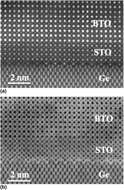
The integration of dissimilar materials is highly desirable for many different types of device applications but often challenging to achieve in practice. The unrivalled imaging capabilities of the aberration-corrected electron microscope enable enhanced insights to be gained into the atomic arrangements across heterostructured interfaces. This paper provides an overview of our recent observations of oxide-semiconductor heterostructures using aberration-corrected high-angle annular-dark-field and large-angle bright-field imaging modes. The perovskite oxides studied include strontium titanate, barium titanate, and strontium hafnate, which were grown on Si(001) and/or Ge(001) substrates using the techniques of molecular-beam epitaxy or atomic-layer deposition. The oxide layers displayed excellent crystallinity and sharp, abrupt interfaces were observed with no sign of any amorphous interfacial layers. The Ge(001) substrate surfaces invariably showed both 1× and 2× periodicity consistent with preservation of the 2 × 1 surface reconstruction following oxide growth. Overall, the results augur well for the future development of functional oxide-based devices integrated on semiconductor substrates.
Contributing Editor: Thomas Walther