Hostname: page-component-745bb68f8f-s22k5 Total loading time: 0 Render date: 2025-01-14T19:07:46.077Z Has data issue: false hasContentIssue false

Single process CVD growth of hBN/Graphene heterostructures on copper thin films

Published online by Cambridge University Press:  27 November 2018

Gene Siegel*
Affiliation:
KBRwyle, Beavercreek, Ohio 45433, USA; and Sensors Directorate, Air Force Research Laboratories, Wright Patterson AFB, Ohio 45433, USA
Gordon Grzybowski
Affiliation:
KBRwyle, Beavercreek, Ohio 45433, USA; and Sensors Directorate, Air Force Research Laboratories, Wright Patterson AFB, Ohio 45433, USA
Timothy Prusnick
Affiliation:
KBRwyle, Beavercreek, Ohio 45433, USA; and Sensors Directorate, Air Force Research Laboratories, Wright Patterson AFB, Ohio 45433, USA
Michael Snure
Affiliation:
Sensors Directorate, Air Force Research Laboratories, Wright Patterson AFB, Ohio 45433, USA
*
a)Address all correspondence to this author. e-mail: gene.siegel.ctr@us.af.mil
Get access

Abstract

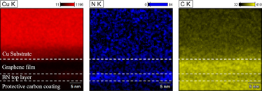
In this study, we have successfully grown hBN/graphene heterostructures on copper thin films using chemical vapor deposition in a single process. The first and most surprising result is that graphene grows underneath hBN and adjacent to the Cu film even though it is deposited second. This was determined from cross-sectional TEM analysis and XPS depth profiling, which chemically identified the relative positions of hBN and graphene. The effect of various growth conditions on graphene/hBN heterostructures was also studied. It was found that a pressure of 200 torr and a hydrogen flow rate of 200 sccm (∼1 H2/N2) yielded the highest quality of graphene, with full surface coverage occurring after a growth time of 120 min. The resulting graphene films were found to be approximately 6–8 layers thick. The grain size of the nanocrystalline graphene was found to be 15–50 nm varying based on growth conditions.

Type
Article
Copyright
Copyright © Materials Research Society 2018 

Access options

Get access to the full version of this content by using one of the access options below. (Log in options will check for institutional or personal access. Content may require purchase if you do not have access.)

References

REFERENCES

Michel, K. and Verberk, B.: Theoretical phonon dispersion in monolayers and multilayers of hexagonal boron-nitride. Phys. Status Solidi 246, 2802 (2009).CrossRefGoogle Scholar
Ishigami, M., Chen, J.H., Cullen, W.G., Fuhrer, M.S., and Williams, E.D.: Atomic structure of graphene on SiO2. Nano Lett. 7, 1643 (2007).CrossRefGoogle ScholarPubMed
Chen, J.H., Jang, C., Xiao, S., Ishigami, M., and Fuhrer, M.: Intrinsic and extrinsic performance limits of graphene devices on SiO2. Nat. Nanotechnol. 3, 206209 (2008).CrossRefGoogle ScholarPubMed
Lee, K.H., Shin, H.J., Lee, J., Lee, I., Kim, G.H., Choi, J.Y., and Kim, S.W.: Large-scale synthesis of high-quality hexagonal boron nitride nanosheets for large-area graphene electronics. Nano Lett. 12, 714718 (2012).CrossRefGoogle ScholarPubMed
Kim, S.M., Hsu, A., Park, M.H., Chae, S.H., Yun, S.J., Lee, J.S., Cho, D.H., Fang, W., Lee, C., Palacios, T., Dresselhaus, M., Kim, K.K., Lee, Y.H., and Kong, J.: Synthesis of large-area multilayer hexagonal boron nitride for high material performance. Nat. Commun. 6, 8662 (2015).CrossRefGoogle ScholarPubMed
Dean, C.R., Young, A.F., Meric, L., Lee, C., Wang, L., Sorgenfrei, S., Watanabe, K., Taniguchi, T., Kim, P., and Shepard, K.L.: Boron nitride substrates for high-quality graphene electronics. J. Nat. Nanotechnol. 5, 722726 (2010).CrossRefGoogle ScholarPubMed
Mayorov, A.S., Gorbachev, R.V., Morozov, S.V., Britnell, L., Jalil, R., Ponomarenko, L.A., Blake, P., Novoselov, K.S., Watanabe, K., Taniguchi, T., and Geim, A.K.: Micrometer-scale ballistic transport in encapsulated graphene at room temperature. Nano Lett. 11, 23962399 (2011).CrossRefGoogle ScholarPubMed
Yang, W., Chen, G., Shi, Z., Liu, C.C., Zhang, L., Xie, G., Cheng, M., Wang, D., Yang, R., Shi, D., Watanabe, K., Tanigushi, T., Yao, Y., Zhang, Y., and Zhang, G.: Epitaxial growth of single domain graphene on hexagonal boron nitride. Nat. Mater. 12, 792797 (2013).CrossRefGoogle ScholarPubMed
Tang, S., Wang, H., Zhang, Y., Li, A., Xie, H., Liu, X., Liu, L., Li, T., Huang, F., Xie, X., and Jiang, M.: Precisely aligned graphene grown on hexagonal boron nitride by catalyst free chemical vapor deposition. Sci. Rep. 3, 2666 (2013).CrossRefGoogle ScholarPubMed
Dabrowski, J., Lippert, G., Schroeder, T., and Lupina, G.: Role of defects in the process of graphene growth on hexagonal boron nitride from atomic carbon. Appl. Phys. Lett. 105, 191610 (2014).CrossRefGoogle Scholar
Plaut, A.S., Wurstbauer, U., Wang, S., Levy, A.L., dos Santos, L.F., Wang, L., Pfeiffer, L.N., Watanabe, K., Taniguchi, T., Dean, C.R., Hone, J., Pinczuk, A., and Garcia, J.M.: Exceptionally large migration length of carbon and topographically-facilitated self-limiting molecular beam epitaxial growth of graphene on hexagonal boron nitride. Carbon 114, 579584 (2017).CrossRefGoogle Scholar
Davies, A., Albar, J.D., Summerfield, A., Thomas, J.C., Cheng, T.S., Korolkov, V.V., Stapleton, E., Wrigley, J., Goodey, N.L., Mellor, C.J., Khlobystov, A.N., Watanabe, K., Taniguchi, T., Foxon, C.T., Eaves, L., Novikov, S.V., and Beton, P.H.: Lattice-matched epitaxial graphene grown on boron nitride. Nano Lett. 18, 149504 (2018).CrossRefGoogle ScholarPubMed
Mishra, N., Miseikis, V., Convertino, D., Gemmi, M., Piazza, V., and Coletti, C.: Rapid and catalyst-free van der Waals epitaxy of graphene on hexagonal boron nitride. Carbon 96, 497502 (2016).CrossRefGoogle Scholar
Tang, S., Wang, H., Wang, H.S., Sun, Q., Zhang, X., Cong, C., Xie, H., Liu, X., Zhuo, X., Huang, F., Chen, X., Yu, T., Ding, F., Xie, X., and Jiang, M.: Silane-catalysed fast growth of large single-crystal graphene on hexagonal boron nitride. Nat. Commun. 6, 6499 (2015).CrossRefGoogle Scholar
Wang, M., Jang, S.K., Jang, W.J., Kim, M., Park, S.Y., Kim, S.W., Kahng, S.J., Choi, J.Y., Ruoff, R.S., Song, Y.J., and Lee, S.: A platform for large-scale graphene electronics-CVD growth of single-layer graphene on CVD grown hexagonal boron nitride. Adv. Mater. 25, 27462752 (2013).CrossRefGoogle ScholarPubMed
Zuo, Z., Xu, Z., Zheng, R., Khanaki, A., Zheng, J.G., and Liu, J.: In situ epitaxial growth of graphene/h-BN van der Waals heterostructures by molecular beam epitaxy. Sci. Rep. 5, 14760 (2015).CrossRefGoogle Scholar
Zheng, R., Khanaki, A., Tian, H., He, Y., Cui, Y., Xu, Z., and Liu, J.: Precipitation growth of graphene under exfoliated hexagonal boron nitride to form heterostructures on cobalt substrate by molecular beam epitaxy. Appl. Phys. Lett. 111, 011903 (2017).CrossRefGoogle Scholar
Davies, A., Albar, J.D., Summerfield, A., Thomas, J.C., Cheng, T.S., Korolkov, V.V., Stapleton, E., Wrigley, J., Goodey, N.L., Mellor, C.J., Khlobystov, A.N., Watanabe, K., Taniguchi, T., Foxon, C.T., Eaves, L., Novikov, S.V., and Beton, P.H.: Lattice-matched epitaxial graphene grown on boron nitride. Nano Lett. 18, 498504 (2018).CrossRefGoogle ScholarPubMed
Zhang, C., Zhao, S., Jin, C., Koh, A.L., Zhou, Y., Xu, W., Li, Q., Xiong, Q., Peng, H., and Liu, Z.: Direct growth of large-area graphene and boron nitride heterostructures by a co-segregation method. Nat. Commun. 6, 6519 (2015).CrossRefGoogle ScholarPubMed
Gao, T., Song, X., Du, H., Nie, Y., Chen, Y., Ji, Q., Sun, J., Yang, Y., Zhang, Y., and Liu, Z.: Temperature-triggered chemical switching growth of in-plane and vertically stacked graphene-boron nitride heterostructures. Nat. Commun. 6, 6835 (2015).CrossRefGoogle ScholarPubMed
Siegel, G., Ciobanu, C.V., Narayanan, B., Snure, M., and Badescu, S.C.: Heterogeneous pyrolysis: A route for epitaxial growth of hBN atomic layers on copper using separate boron and nitrogen precursors. Nano Lett. 4, 24042413 (2017).CrossRefGoogle Scholar
Song, L., Lu, H., Sorokin, P.B., Jin, C., Ni, J., Kvashnin, A.G., Kvashnin, D.G., Lou, J., Yakobson, B.I., and Ajayan, P.M.: Large scale growth and characterization of atomic hexagonal boron nitride layers. Nano Lett. 10, 32093215 (2010).CrossRefGoogle ScholarPubMed
Moulder, J.F., Stickle, W.F., Sobol, P.E., and Bombem, D.: Handbook of X-Ray Photoelectron Spectroscopy, Chastain, J., ed. (Perkin Elmer Co., Eden Prairie, Minnesota, 1992); p. 54.Google Scholar
Gorbachev, R.V., Riaz, I., Nair, R.R., Jalil, R., Britnell, L., Belle, B.D., Hill, E.W., Novoselov, K.S., Watanabe, K., Taniguchi, T., Geim, A.K., and Blake, P.: Hunting for monolayer boron nitride: Optical and Raman signatures. Small 7, 465468 (2011).CrossRefGoogle ScholarPubMed
Joshi, S., Ecija, D., Koitz, R., Iannuzzi, M., Seitsonen, A.P., Hutter, J., Sachdev, H., Vijayaraghavan, S., Bischoff, F., Seufert, K., Barth, J.V., and Auwarter, W.: Boron nitride on Cu(111): An electronically corrugated monolayer. Nano Lett. 12, 58215828 (2012).CrossRefGoogle ScholarPubMed
Liu, Z., Song, L., Zhao, S., Huang, J., Ma, L., Zhang, J., Lou, J., and Ajayan, P.M.: Direct growth of graphene/hexagonal boron nitride stacked layers. Nano Lett. 11, 20322037 (2011).CrossRefGoogle ScholarPubMed
Hwang, J., Kim, M., Campbell, D., Alsalman, H.A., Kwak, J.Y., Shivaraman, S., Woll, A.R., Shigh, A.K., Hennig, R.G., Corantla, S., Rummeli, M.H., and Spencer, M.G.: van der Waals epitaxial growth of graphene on sapphire by chemical vapor deposition without a metal catalyst. ACS Nano 7, 385395 (2013).CrossRefGoogle Scholar
Oliveira, M.H., Schumann, T., Garallo-Caballero, R., Fromm, F., Seyller, T., Ramsteiner, M., Trampert, A., Geelhaar, L., Lopes, J.M.J., and Riechert, H.: Mono and few-layer nanocrystalline graphene grown on Al2O3 (0001) by molecular beam epitaxy. Carbon 56, 339350 (2013).CrossRefGoogle Scholar
Zemlyanov, D.Y., Jespersen, M., Zakharov, D.N., Hu, J., Paul, R., Kumar, A., Pacley, S., Glavin, N., Saenz, D., Smith, K.C., Fisher, T.S., and Voevodin, A.A.: Versatile technique for assessing thickness of 2D layered materials by XPS. Nanotechnology 29, 115705 (2018).CrossRefGoogle ScholarPubMed