Hostname: page-component-745bb68f8f-v2bm5 Total loading time: 0 Render date: 2025-01-14T19:03:58.693Z Has data issue: false hasContentIssue false

Size effects on stress relaxation across the metal–insulator transition in VO2 thin films

Published online by Cambridge University Press:  03 June 2011
Viswanath Balakrishnan
Affiliation:
Harvard School of Engineering and Applied Sciences, Harvard University, Cambridge, Massachusetts 02138
Changhyun Ko
Affiliation:
Harvard School of Engineering and Applied Sciences, Harvard University, Cambridge, Massachusetts 02138
Shriram Ramanathan*
Affiliation:
Harvard School of Engineering and Applied Sciences, Harvard University, Cambridge, Massachusetts 02138
*
a)Address all correspondence to this author. e-mail: shriram@seas.harvard.edu
Get access

Abstract

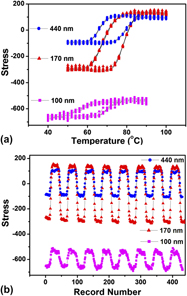
We report on in situ stress relaxation behavior of vanadium dioxide thin films across the thermally driven metal–insulator transition (MIT) and size effects. Although the residual stress follows an inverse relationship with film thickness, the metal–insulator phase transition-induced stress varies nonmonotonically with increase in film thickness and grain size. Maximum transformation stress of −447 MPa is observed across the MIT for ∼170-nm-thick film with an average grain size of ∼70 nm. The interplay between constraint effects and nanostructure leads to nontrivial stress relaxation trends and provides insights into design of phase transition materials for switching devices.

Type
Materials Communications
Copyright
Copyright © Materials Research Society 2011

Access options

Get access to the full version of this content by using one of the access options below. (Log in options will check for institutional or personal access. Content may require purchase if you do not have access.)

References

REFERENCES

1.Morin, F.J.: Oxides which show a metal-to-insulator transition at the Neel temperature. Phys. Rev. Lett. 3(1), 34 (1959).Google Scholar
2.Dong-Wook, O., Changhyun, K., Shriram, R., and Cahill, D.G.: Thermal conductivity and dynamic heat capacity across the metal-insulator transition in thin film VO2. Appl. Phys. Lett. 96(15), 151906 (2010).Google Scholar
3.Barker, A.S., Verleur, H.W., and Guggenheim, H.J.: Infrared optical properties of vanadium dioxide above and below the transition temperature. Phys. Rev. Lett. 17(26), 1286 (1966).CrossRefGoogle Scholar
4.Viswanath, B., Ko, Changhyun, and Ramanathan, Shriram: Thermoelastic switching with controlled actuation in VO2 thin films. Scr. Mater. 64(6), 490 (2011).Google Scholar
5.Rua, A., Fernandez, F.E., and Sepulveda, N.: Bending in VO2-coated microcantilevers suitable for thermally activated actuators. J. Appl. Phys. 107(7), 074506 (2010).Google Scholar
6.Kang, M.J., Choi, S.Y., Wamwangi, D., Wang, K., Steimer, C., and Wuttig, M.: Structural transformation of SbxSe100-x thin films for phase change nonvolatile memory applications. J. Appl. Phys. 98(1), 014904 (2005).Google Scholar
7.Lopez, R., Haynes, T.E., Boatner, L.A., Feldman, L.C., and Haglund, R.F. Jr.: Size effects in the structural phase transition of VO2 nanoparticles. Phys. Rev. B 65(22), 224113 (2002).Google Scholar
8.Lopez, R., Feldman, L.C., and Haglund, R.F.: Size-dependent optical properties of VO2 nanoparticle arrays. Phys. Rev. Lett. 93(17), 177403 (2004).Google Scholar
9.Sahana, M.B., Dharmaprakash, M.S., and Shivashankar, S.A.: Microstructure and properties of VO2 thin films deposited by MOCVD from vanadyl acetylacetonate. J. Mater. Chem. 12(2), 333 (2002).CrossRefGoogle Scholar
10.Brassard, D., Fourmaux, S., Jean-Jacques, M., Kieffer, J.C., and El Khakani, M.A.: Grain size effect on the semiconductor-metal phase transition characteristics of magnetron-sputtered VO2 thin films. Appl. Phys. Lett. 87(5), 051910 (2005).Google Scholar
11.Suh, J.Y., Lopez, R., Feldman, L.C., and Haglund, R.F. Jr.: Semiconductor to metal phase transition in the nucleation and growth of VO2 nanoparticles and thin films. J. Appl. Phys. 96(2), 1209 (2004).Google Scholar
12.Thompson, V.C. and Carel, R.: Stress and grain growth in thin films. J. Mech. Phys. Solids 44(5), 657 (1996).Google Scholar
13.Waitz, T., Antretter, T., Fischer, F.D., Simha, N., and Karnthaler, H.: Size effects on the martensitic phase transformation of NiTi nanograins. J. Mech. Phys. Solids 55(2), 419 (2007).Google Scholar
14.Dai, L., Cao, C., Gao, Y., and Luo, H.: Synthesis and phase transition behavior of undoped VO2 with a strong nano-size effect. Sol. Energy Mater. Sol. Cells 95(2), 712 (2011).CrossRefGoogle Scholar
15.Donev, E.U., Ziegler, J.I., Haglund, R.F. Jr., and Feldman, L.C.: Size effects in the structural phase transition of VO2 nanoparticles studied by surface-enhanced Raman scattering. J. Opt. A: Pure Appl. Opt. 11, 125002 (2009).Google Scholar
16.Ishida, A. and Sato, M.: Thickness effect on shape memory behavior of Ti-50.0at.%Ni thin film. Acta Mater. 51(18), 5571 (2003).Google Scholar