Hostname: page-component-78c5997874-m6dg7 Total loading time: 0 Render date: 2024-11-13T03:02:50.622Z Has data issue: false hasContentIssue false

Vertical graphene by plasma-enhanced chemical vapor deposition: Correlation of plasma conditions and growth characteristics

Published online by Cambridge University Press:  23 October 2013

Emil Sandoz-Rosado
Affiliation:
Center for Nanotechnology, NASA Ames Research Center, Moffett Field, California 94035
William Page
Affiliation:
Center for Nanotechnology, NASA Ames Research Center, Moffett Field, California 94035
David O’Brien
Affiliation:
Center for Nanotechnology, NASA Ames Research Center, Moffett Field, California 94035
Joshua Przepioski
Affiliation:
Center for Nanotechnology, NASA Ames Research Center, Moffett Field, California 94035
Dennis Mo
Affiliation:
Center for Nanotechnology, NASA Ames Research Center, Moffett Field, California 94035
Benjamin Wang
Affiliation:
Center for Nanotechnology, NASA Ames Research Center, Moffett Field, California 94035
Tam-Triet Ngo-Duc
Affiliation:
Center for Nanotechnology, NASA Ames Research Center, Moffett Field, California 94035
Jovi Gacusan
Affiliation:
Center for Nanotechnology, NASA Ames Research Center, Moffett Field, California 94035
Michael W. Winter
Affiliation:
Center for Nanotechnology, NASA Ames Research Center, Moffett Field, California 94035
M. Meyyappan
Affiliation:
Center for Nanotechnology, NASA Ames Research Center, Moffett Field, California 94035
Robert D. Cormia
Affiliation:
Foothill College and UCSC/NASA-ARC Advanced Studies Laboratories, NASA Ames Research Center, Moffett Field, California 94035
Shuhei Takahashi
Affiliation:
Center for Nanotechnology and UCSC/NASA-ARC Advanced Studies Laboratories, NASA Ames Research Center, Moffett Field, California 94035; and Department of Electrical Engineering, University of California Santa Cruz, Santa Cruz, California 95064
Michael M. Oye*
Affiliation:
Center for Nanotechnology and UCSC/NASA-ARC Advanced Studies Laboratories, NASA Ames Research Center, Moffett Field, California 94035; and Department of Electrical Engineering, University of California Santa Cruz, Santa Cruz, California 95064
*
a)Address all correspondence to this author. e-mail: Michael.M.Oye@nasa.gov
Get access

Abstract

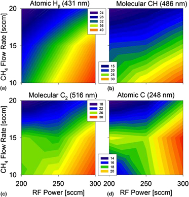
Vertically aligned graphene was grown by plasma-enhanced chemical vapor deposition using methane feedstock. Optical emission spectroscopy (OES) was used to monitor the plasma species, and Raman spectroscopy was used for characterizing the properties of as-grown vertically aligned graphene. OES-derived information on plasma species, such as C, C2, CH, and H, are correlated with the properties of the vertically aligned graphene. Graphene grown at 250 W and 15 sccm exhibited the lowest amount of defects. Although OES peak intensities occurred at the highest power and lowest flow conditions, the OES peak ratios of plasma species had a greater dependence on flow rate and exhibited a saddle point in the atomic C/H ratio corresponding to optimal growth involving the lowest amount of overall defects. Plasma diagnostics provides a valuable approach to optimize growth characteristics and material properties.

Type
Invited Papers
Copyright
Copyright © Materials Research Society 2013 

Access options

Get access to the full version of this content by using one of the access options below. (Log in options will check for institutional or personal access. Content may require purchase if you do not have access.)

References

REFERENCES

Choi, W.B. and Lee, J.W.: Graphene: Synthesis and Applications (CRC Press, Boca Raton, FL, 2012).Google Scholar
Zhu, Y., Murali, S., Cai, W.W., Li, X.S., Suk, J.W., Potts, J.R., and Ruoff, R.S.: Graphene and graphene oxide: Synthesis, properties and applications. Adv. Mater. 22, 3906 (2010).Google Scholar
Rümmeli, M.H., Rocha, C.G., Ortmann, F., Ibrahim, I., Sevincli, H., Börrnert, F., Kuntsmann, J., Backmatiuk, A., Potschke, M., Shiraishi, M., Meyyappan, M., Buchner, B., Roche, S., and Cuniberti, G.: Graphene: Piecing it together. Adv. Mater. 23, 4471 (2011).Google Scholar
Yu, Q., Lian, J., Siriponglert, S., Li, H., Chen, Y.P., and Pei, S.S.: Graphene segregated on Ni surfaces and transferred to insulators. Appl. Phys. Lett. 93, 113103 (2008).CrossRefGoogle Scholar
De Arco, L.G., Zhang, Y., Kumar, A., and Zhou, C.: Synthesis, transfer, and devices of single- and few-layer graphene by chemical vapor deposition. IEEE Trans. Nanotechnol. 8, 135 (2009).CrossRefGoogle Scholar
Lee, B.J., Yu, H.Y., and Jeong, G.H.: Controlled synthesis of monolayer graphene toward transparent flexible conductive film application. Nanoscale Res. Lett. 5, 1768 (2010).Google Scholar
Rummeli, M.H., Bachmatiuk, A., Scott, A., Bornett, F., Warner, J.H., Hoffman, V., Lin, J.H., Cunibert, G., and Buckner, B.: Direct lower-temperature nanographene CVD synthesis over a dielectric insulator. ACS Nano 4, 4206 (2013).Google Scholar
Hiramatsu, M., Shiji, K., Amano, H., and Hori, M.: Fabrication of vertically aligned carbon nanowalls using capacitively coupled plasma-enhanced chemical vapor deposition assisted by hydrogen radical injection. Appl. Phys. Lett. 84, 4708 (2004).Google Scholar
Hiramatsu, M. and Hori, M.: Fabrication of carbon nanowalls using novel plasma processing. Jpn. J. Appl. Phys. 45, 5522 (2006).CrossRefGoogle Scholar
Wang, J.J., Zhu, M.Y., Outlaw, R.A., Zhao, X., Manos, D.M., Holloway, B.C., and Mammana, V.P.: Free-standing subnanometer graphite sheets. Appl. Phys. Lett. 85, 1265 (2004).Google Scholar
Wang, J.J., Zhu, M., Outlaw, R.A., Zhao, X., Manos, D.M., and Holloway, B.C.: Synthesis of carbon nanosheets by inductively coupled radio-frequency plasma enhanced chemical vapor deposition. Carbon 42, 2867 (2004).CrossRefGoogle Scholar
Zhu, M., Wang, J.J., Holloway, B.C., Outlaw, R.A., Zhao, X., Hou, K., Shutthanandan, V., and Manos, D.M.: A mechanism for carbon nanosheet formation. Carbon 45, 2229 (2009).Google Scholar
Malesevic, A., Vitchev, R., Schouteden, K., Volodin, A., Zhang, L., and Tendeloo, G.V.: Synthesis of few-layer graphene via microwave plasma-enhanced chemical vapour deposition. Nanotechnology 19, 305604 (2008).Google Scholar
Chatei, H., Belmahi, M., Assouar, M.B., Le Brizoual, L., Bourson, P., and Bougdira, J.: Growth and characterization of carbon nanostructures obtained by MPACVD system using CH4/CO2 gas mixture. Diamond Relat. Mater. 15, 1041 (2006).CrossRefGoogle Scholar
French, B.L., Wang, J.J., Zhu, M.Y., and Holloway, B.C.: Evolution of structure and morphology during plasma-enhanced chemical vapor deposition of carbon nanosheets. Thin Solid Films 494, 105 (2006).Google Scholar
Teii, K., Shimada, S., Nakashima, M., and Chuang, A.T.H.: Synthesis and electrical characterization of n-type carbon nanowalls. J. Appl. Phys. 106, 084303 (2009).CrossRefGoogle Scholar
Yuan, G.D., Zhang, W.J., Yang, Y., Yang, Y.B., Li, Y.Q., Wang, J.X., Meng, X.M., He, Z.B., Wu, C.M.L., Belloy, I., Lee, C.S., and Lee, S.T.: Graphene sheets via microwave chemical vapor deposition. Chem. Phys. Lett. 467, 361 (2009).Google Scholar
Meyyappan, M.: Plasma nanotechnology: Past, present and the future. J. Phys. D: Appl. Phys. 44, 174002 (2011).Google Scholar
Meyyappan, M. and Lee, J.S.: Graphene growth by plasma-enhanced chemical vapor deposition (PECVD), in Plasma Processing of Nanomaterials, edited by Sankaran, R.M. (CRC Press, Boca Raton, FL, 2012).Google Scholar
Hiramatsu, M., Kihashi, Y., Kondo, H., and Hori, M.: Nucleation control of carbon nanowalls using inductively coupled plasma-enhanced chemical vapor deposition. Jpn. J. Appl. Phys. 52, 01AK05 (2013).Google Scholar
Losurdo, M., Giangregorio, M.M., Capezzuto, P., and Bruno, G.: Graphene CVD growth on copper and nickel: Role of hydrogen in kinetics and structure. Phys. Chem. Chem. Phys. 13, 20836 (2011).Google Scholar
Kim, Y.S., Lee, J.H., Kim, Y.D., Jerng, S-K., Joo, K., Kim, E., Jung, J., Yoon, E., Park, Y.D., Seo, S., and Chun, S-H.: Methane as an effective hydrogen source for single-layer graphene synthesis on Cu foil by plasma enhanced chemical vapor deposition. Nanoscale 5, 1221 (2013).Google Scholar
Levchenko, I., Ostrikov, K., Rider, A.E., Tam, E., Vladimirov, S.V., and Xu, S.: Growth kinetics of carbon nanowall-like structures in low temperature plasmas. Phys. Plasmas 14, 063502 (2007).Google Scholar
Hash, D.B. and Meyyappan, M.: Model based comparison of thermal and plasma chemical vapor deposition of carbon nanotubes. J. Appl. Phys. 93, 750 (2003).Google Scholar
Cruden, B.A., Cassell, A.M., Hash, D.B., and Meyyappan, M.: Residual gas analysis of a dc plasma for carbon nanofiber growth. J. Appl. Phys. 96, 5284 (2004).Google Scholar
Hash, D.B., Bell, M.S., Teo, K.B.K., Cruden, B.A., Milne, W.I., and Meyyappan, M.: An investigation of plasma chemistry for DC plasma enhanced chemical vapour deposition, of carbon nanotubes and nanofibers. Nanotechnology 16, 925 (2005).CrossRefGoogle Scholar
Cruden, B.A. and Meyyappan, M.: Characterization of a radio frequency carbon nanotube growth plasma by ultraviolet adsorption and optical emission spectroscopy. J. Appl. Phys. 97, 084311 (2005).Google Scholar
Oye, M.M., Mattord, T.J., Hallock, G.A., Bank, S.R., Wistey, M.A., Reifsnider, J.M., Ptak, A.J., Yuen, H.B., Harris, J.S. Jr., and Holmes, A.L. Jr.: Effects of different plasma species (atomic N, metastable N2*, and ions) on the optical properties of dilute nitride materials grown by plasma-assisted molecular beam epitaxy. Appl. Phys. Lett. 91, 191903 (2007).CrossRefGoogle Scholar
Oye, M.M., Bank, S.R., Ptak, A.J., Reedy, R.C., Goorsky, M.S., and Holmes, A.L. Jr.: Role of ion damage on unintentional Ca incorporation during the plasma-assisted molecular-beam epitaxy growth of dilute nitrides using N(2)/Ar source gas mixtures. J. Vac. Sci. Technol., B 26, 1058 (2008).Google Scholar
Miller, P.A., Hebner, G.A., Greenberg, K.E., Pochan, P.D., and Aragon, B.P.: An inductively-coupled plasma source for the gaseous electronics conference rf reference cell. J. Res. Nat. Inst. Stand. Technol. 100, 427 (1995).Google Scholar
Ostrikov, K., Neyts, E.C., and Meyyappan, M.: Plasma nanoscience: From nano-solids in plasmas to nano-plasmas in solids. Adv. Phys. 62, 113 (2013).Google Scholar
Delzeit, L., McAninch, I., Cruden, B.A., Hash, D., Chen, B., Han, J., and Meyyappan, M.: Growth of multiwall carbon nanotubes in an inductively coupled plasma reactor. J. Appl. Phys. 9, 6027 (2002).Google Scholar
Vizireanu, S., Stoica, S.D., Luculescu, C., Nistor, L.C., Mitu, B., and Dinescu, G.: Plasma techniques for nanostructured carbon materials synthesis. A case study: Carbon nanowall growth by low pressure expanding RF plasma. Plasma Sources Sci. Technol. 19 034016 (2010).Google Scholar
Mori, S. and Suzuki, M.: Non-catalytic, low-temperature synthesis of carbon nanofibers by plasma-enhanced chemical vapor deposition. In Nanofibers, edited by Kumar, A. (InTech, Rijeka, Croatia, 2010).Google Scholar
Al-Shboul, K.F., Harilal, S.S., Hassanein, A., and Polek, M.: Dynamics of C2 formation in laser-produced carbon plasma in helium environment. J. Appl. Phys. 109, 053302 (2011).Google Scholar
Gottscho, R.A. and Donnelly, V.M.: Optical-emission actinometry and spectral-line shapes in RF glow discharges. J. Appl. Phys. 56, 245 (1984).Google Scholar
Ferrari, A.C., Meyer, J.C., Scardaci, V., Casiraghi, C., Lazzeri, M., Mauri, F., Piscanec, S., Jiang, D., Novoselov, K.S., Roth, S., and Geim, A.K.: Raman spectrum of graphene and graphene layers. Phys. Rev. Lett. 97, 187401 (2006).Google Scholar
Vizireanu, S., Ionita, M.D., Dinescu, G., Enculescu, I., Baibarac, M., and Baltog, I.: Post-synthesis carbon nanowalls transformation under hydrogen, oxygen, nitrogen, tetrafluoroethane and sulfur hexafluoride plasma treatments. Plasma Processes Polym. 9, 363370 (2012).Google Scholar
Rao, C.N.R., Sood, A.K., Subrahmanyam, K.S., and Govindaraj, A.: Graphene: The new two-dimensional nanomaterial. Angew. Chem. Int. Ed. 48, 7752 (2009).Google Scholar
Lv, R., Li, Q., Botello-Mendez, A.R., Hayashi, T., Wang, B., Berkdemir, A., Hao, Q., Elıas, A.L., Cruz-Silva, R., Gutierrez, H.R., Kim, Y.A., Muramatsu, H., Zhu, J., Endo, M., Terrones, H., Charlier, J-C., Pan, M., and Terrones, M.: Nitrogen-doped graphene: Beyond single substitution and enhanced molecular sensing. Sci. Rep. 2, 586 (2012).Google Scholar
Cancado, L.G., Jorio, A., Martins Ferreira, E.H., Stavale, F., Achete, C.A., Capaz, R.B., Moutinho, M.V.O., Lombardo, A., Kulmala, T.S., and Ferrari, A.C.: Quantifying defects in graphene via Raman spectroscopy at different excitation energies. Nano Lett. 11, 31903196 (2011).Google Scholar
Meyyappan, M., Delzeit, L., Cassell, A., and Hash, D.: Carbon nanotube growth by PECVD: A review. Plasma Sources Sci. Technol. 12, 205 (2003).Google Scholar