I. Introduction
Recently, the semiconductor gallium nitride (GaN) has been recognized for several decades for their potential and, recently, commercial viability in wide band optoelectronic device applications [Reference Egawa, Jimbo and Umeno1]. The electronic devices that can be used for high power and high temperature applications have also been fabricated, among which GaN-based MOSFETs are actively studied [Reference Ren, Hong, Chu, Marcus, Schurman and Baca2]. The traditional GaN MOS structures fabricated with conventional oxides, like SiO2 [Reference Arulkmaran, Jimbo, Ishikawa, Arulkumaran and Egawa3,Reference Casey, Gfoutain, Alley, Keller and DenBarrs4], Si3N4 [Reference Arulkmaran, Jimbo, Ishikawa, Arulkumaran and Egawa3], Ga2O3(Gd2O3) [Reference Casey, Gfoutain, Alley, Keller and DenBarrs4], as insulators have to be improved. One important reason is that large applied voltage, which is incompatible with most other electronic devices, is imposed on all the previous GaN MOS structures. In our work, ferroelectric oxides have been used in GaN MOS structures to address this problem because of large polarization provided by ferroelectric and the high dielectric constant of ferroelectric gate.
Since the field-effect transistors (MFSFETs) was first proposed by Wu [Reference Wu5, Reference Wu6], it has been extensively studied because of their applications in non-volatility and high speed memories and integration circuits [Reference Rost, Lin and Rabson7-Reference Kijima and Matsunaga10]. Nowadays, the semiconductor used in metal-ferroelectric-semiconductor (MFS) structures usually is Si. The instability of the ferroelectric/Si interface due to interdiffusion between ferroelectrics and Si substrates has still impeded the development of the novel device [Reference Alexe8]. Consequently, many kinds of buffer layers have been deposited between ferroelectrics and Si substrates to prevent the behavior of interdiffusion [Reference Senzaki, Kurihara, Nomura, Mitsunaga, Iwasaki and Ueno11-Reference Lee, Choi and Lee13], which also decreases the control of ferroelectric polarization on the potential of Si surface. GaN is so stable that it can work without weight loss at 1000 0C[Reference Morimoto14]. GaN MFS structure is a good candidate to develop ferroelectric/semiconductor interface and MFSFETs with high-temperature stability.
II. Experiments
In the GaN MFS structure developed in this work, n-type GaN active layer is grown by light radiant heating low-pressure metalorganic chemical vapor deposition (LRH-LP-MOCVD) on the (0001) oriented sapphire (Al2O3) substrate which is pre-cleaned by organic solvents and H2SO4 : H3PO3(3:1) solutions [Reference Shen, Zhou, Chen, Chen, Zang, Zhang, Shi and Zheng15,Reference Zhou, Shen, Chen, Chen, Zhang, Shi and Zheng16]. Before the epitaxial growth of GaN layer, a thin GaN buffer (about 30nm) was deposited at 520 0C on sapphire substrate. Then the GaN active layer (n∼1017cm−3) was deposited at 1040 0C. Afterwards, the ferroelectric Pb(Zr0.53Ti0.47)O3 (PZT) films with different thickness have been deposited directly on GaN films by pulsed laser deposition (PLD). The experimental condition is showed in the Table 1.
Table I. The experimental condition in the deposition of PZT by pulsed laser deposition (PLD)
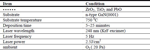
After the deposition of PZT, the samples are annealed in-situ in the chamber with 0.5 atm. O2.for 30 minutes. In the following process, very thin SiO2 films are deposited on thin PZT films (about 130 nm) by plasma enhanced chemical vapor deposition (PECVD) to decrease the leakage current. Then the top electrodes (about 200 nm) are fabricated by magnetron sputtering and patterned with a shadow mask of holes 0.2mm in diameter, while the bottom electrodes are contacted with aluminum (Al) from the edge of GaN top surface. Finally, the whole samples are annealed at the temperature of 600 0C after which excellent ohmic contacts on GaN are formed.
III. Discussion
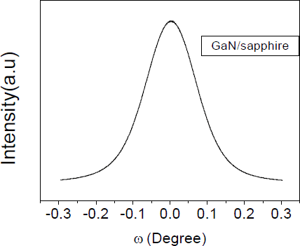
The GaN films deposited by LRH-LP-MOCVD have been characterized by photoluminescence (PL) and high-resolution x-ray diffraction (HRXRD) methods. In the PL spectra, strong band-edge luminescence has been observed and undesirable YL peaks do not exist. The full width at half maximum (FWHM) of GaN in the HRXRD pattern is 8.6 min.
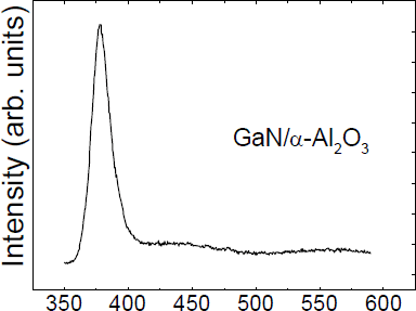
Figure 1 A typical PL spectrum of GaN on sapphire by LRH-LP-MOCVD.
The PZT films directly on GaN (0001) are characterized by X-ray diffraction (XRD). The results show that the PZT films are deposited along the orientations of <100>, <110>, <211> and <111>, among which the <110> peak is the strongest. No undesirable peak of pyrochlore phase appears in the XRD pattern, which shows that PZT films are well crystallized with perovskite structure.

Figure 2 A typical HRXRD spectrum GaN on sapphire grown by LRH-LP-MOCVD.
The high-frequency capacitance-voltage (C-V) measurement is an important characterization method of MOS structures. When the applied bias are large enough to make the GaN surface approach depletion, the bias voltage (Vb ) has been distributed between gate insulator (Vi ) and depletion layer (Vd ):
The GaN MOS structures under the bias can be expressed as the two capacitors, the insulator capacitor (Ci ) and depletion capacitor (Cd ), in series. The voltage and capacitance distributions have the following relationship:

Therefore, the bias voltage can be expressed into the following form:

Figure 3. An X-ray spectrum of PZT directly on GaN (0001) by pulsed laser deposition.
As to a specific semiconductor sample, the Vd is a constant. Therefore, in order to decrease the bias voltage (Vb ), we have to increase the insulator capacitance (Ci ). In traditional GaN MOS structures with SiO2 or Si3N4 as gate oxides, the effort made to decrease the large applied bias has focused on reducing the thickness of gate oxides, which results in the increase of Cd . However, these approaches to decrease the bias voltage are not desirable. It is very difficult to allow GaN to approach inversion under bias of 15 volts although the oxide insulators are thinner than 60nm [Reference Casey, Gfoutain, Alley, Keller and DenBarrs4].
In GaN MFS structures, the insulator capacitance (Ci ) has been greatly increased because of the high dielectric constant of ferroelectrics. By using the ferroelectric oxides as gate insulators, we need not reduce the oxide thickness to increase the capacitance.
Moreover, in the MFS structures, there are polarization fields (on the order of 106 V/cm) much larger than external applied field (on the order of 10−4∼10−5 V/cm) at the ferroelectric/semiconductor interfaces. Figure 4 shows the C-V behavior of the GaN MFS structures with 1 μ PZT films. We can find that the GaN MFS structures with thick gate oxides can approach inversion under the bias of 15 volts.

Figure 4 The C-V behaviors of GaN MFS structures with the 1 μ PZT films. The structures can approach reversion under 15 V, which is better than the C-V behaviors of GaN MOS structures with the same thick SiO2 films.
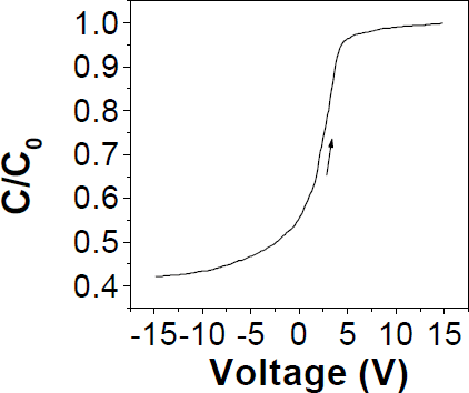
The GaN MFS structures with 100 nm PZT films have also been characterized by high-frequency C-V method. In Figure 5, we can find the applied bias has been decreased sharply. The GaN active layer can approach inversion just under 5V, which can satisfy the practical need of the GaN MOS structures.
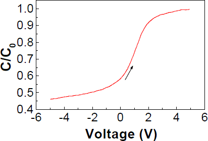
Figure 5 The C-V behaviors of GaN MFS structures with the 100nm PZT films. The structures can approach inversion just under small bias.
IV. Conclusion
In our work, GaN-based metal-ferroelectric-semiconductor (MFS) structures have been fabricated by using the ferroelectric oxide Pb(Zr0.53Ti0.47)O3 as gate insulators. The electrical properties of GaN MFS structures with different oxide thickness have been studied by the high-frequency C-V measurement. Due to the high dielectric constant and large polarization field of PZT films, the large applied voltage on conventional GaN MIS structures has been decreased sharply with comparison to that of traditional GaN MOS structures.


