Introduction
The group III-nitride semiconductors are promising materials for applications in opto-electronic devices such as light emitting diodes and laser diodes [Reference Nakamura, Senoh, Nagahama, Iwasa, Yamada, Matsushita, Kiyoku, Sugimoto, Kozaki, Umemoto, Sano and Chocho1], and in field effect transistors[Reference Vetury, Marchand, Parish, Fini, Ibbetson, Keller, Speck, DenBaars and Mishra2]. Although these devices are fabricated mainly on sapphire substrate, it is not easy to achieve a high performance because of a high dislocation density in the crystal originating from the large differences in lattice constants between GaN and sapphire. An attempt to reduce the dislocation density of crystal using epitaxial lateral overgrowth (ELO) technique was employed in GaAs[Reference Ujiie and Nishinaga3]. Recently, Usui et al. achieved a thick GaN epitaxial layer with a dislocation density as low as 107cm−2 using ELO by hydride vapor phase epitaxy (HVPE) [Reference Usui, Sunakawa, Sakai and Yamaguchi4].
SiO2 or SiNx insulator has been normally used as the mask material for ELO-GaN. Besides those materials, ELO-GaN with tungsten (W) metal mask was investigated to fabricate optical and electronic devices with higher performance. It was reported that the ELO-GaN layers are successfully obtained with the W mask as well as SiO2 or SiNx masks via HVPE and have a better crystalline quality than that with SiO2 mask[Reference Sone, Nambu, Kawaguchi, Yamaguchi, Miyake, Hiramatsu, Iyechika, Maeda and Sawaki5].
In the ELO of GaAs, the W metal mask was employed and the W-buried structure was obtained to fabricate a permeable base transistor (PBT) or static induction transistor (SIT) [Reference Asai, Adachi, Ando and Oe6]. The fabrication of the electronic devices such as PBTs or SITs via the ELO technique in GaN is very attractive for the use as high power and/or high frequency devices under crucial environments such as at high temperature or at highly radioactive environment. Recently, Kawaguchi et al. performed the selective area growth (SAG) of GaN using the W mask by metalorganic vapor phase epitaxy (MOVPE) and achieved high selectivity[Reference Kawaguchi, Nambu, Sone, Yamaguchi, Miyake, Hiramatsu, Miyake and Sawaki7].
In this work, we demonstrate the ELO of GaN using the W mask by MOVPE and obtain the W-buried structure with GaN. The characteristics of ELO-GaN were also investigated by means of atomic force microscopy (AFM) and x-ray rocking curve (XRC).
Experimental Procedure
MOVPE of GaN using a W mask was performed on two types of samples. The sample is a 4.0 μm-thick (0001) GaN epilayer, which had been grown on sapphire (0001) substrate using an GaN low temperature buffer layer by MOVPE. Another sample is a 40-100 nm thick AlGaN epilayer on the 4.0 μm-thick (0001) GaN epilayer. The 30 - 50 nm thick W mask was deposited by electron beam evaporation method. Stripe windows of 2 or 5 µm width with a periodicity of 4 or 10 µm, respectively, were developed in the <1
Results and Discussion
In order to investigate effects of the W mask which affects the underlying GaN and AlGaN layers in hydrogen ambient at a high temperature, we attempted thermal annealing at 500 to 700 °C of GaN and AlGaN with a striped W mask. Consequently, the surface of GaN window regions was roughened, including Ga droplets and GaN whiskers. This phenomenon occurred above 500°C. It is reported that an underlying GaN layer with a striped SiO2 mask is decomposed higher than 900 °C in hydrogen ambient and there is no damage less than 900 °C[Reference Hiramatsu, Matsushima, Hanai and Sawaki9]. Therefore, the W mask works as a catalyst to enhance decomposition of GaN. It is thought that W may produce radical hydrogen that can decompose GaN easily. On the other hand, the surface of AlGaN is not roughened even though the annealing temperature is 700°C. Any Ga droplets and GaN whiskers are not observed on the AlGaN layer. Hence, the catalytic effect of the W mask does not work in the AlGaN layer. Thus, it is found that the top AlGaN layer plays an important role to protect the bottom GaN from decomposition.
The ELO was performed using the W mask with stripe windows of 5 μm width. Figure 1 shows the cross sectional SEM images of ELO GaN with the underlying GaN (a) and AlGaN/GaN (b). About 5 μm-thick ELO GaN layers are obtained in both cases.

Figure 1 The cross sectional SEM photographs of ELO GaN with underlying GaN (a) and AlGaN (b). The width of stripe window is 5 μm.
Large voids occurs under the W mask as seen in Fig.1(a), indicating that the underlying GaN is decomposed during the ELO process owing the catalytic effect of the W mask. On the contrary, there are no voids in Fig.1(b). Therefore, the underlying AlGaN layer can prevent the bottom GaN from being decomposed.
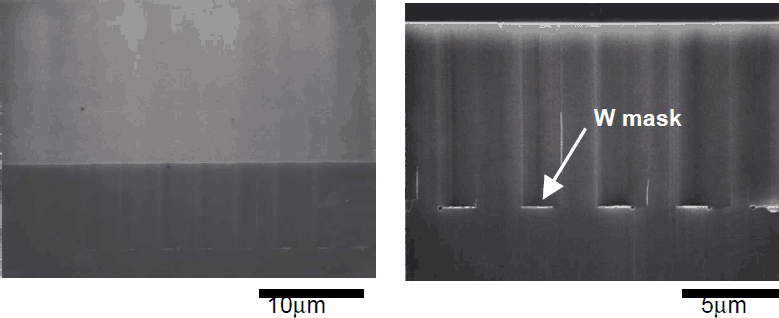
The W masks are not buried completely after the growth process in the case of the 5 μm wide mask. The width of stripe was narrowed to bury the W mask completely. Figure 2 shows the cross sectional SEM images of ELO GaN with the underlying AlGaN/GaN layer. The widths of mask and window are 2 μm and 2 μm, respectively. This result clearly shows that the W mask is buried completely and the surface is smooth.

Figure 2 The cross sectional SEM photographs of ELO GaN with underlying AlGaN. The width of stripe window is 2 μm.
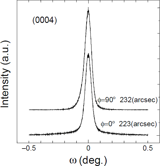
To characterize the surface morphology and the tilting of c-axis of the ELO GaN, we carried out x-ray diffraction and atomic force microscope (AFM). Figure 3 shows the results of AFM for the sample of Fig. 2. In this figure, atomic step structures with 0.1 μm-width and 0.3 nm-height are observed. This means that the step flow growth occurs in the ELO of the GaN layer. Figure 4 shows the XRCs of the (0004) reflection for φ = 0 ° and 90 ° of the ELO GaN layer with the stripe directions of the masks along the direction of <1

Figure 3 The results of AFM for the sample of Fig.2.

Figure 4 The XRCs of the (0004) reflection of the sample of Fig.2.
Conclusion
The two step ELO of GaN using W mask was performed by LP- MOVPE. GaN with a striped W metal pattern is easily decomposed above 500 °C by the W catalytic effect that causes radical hydrogen to attack the GaN layer. It is difficult to bury the W mask because severe damage occurs in the GaN epilayer under the mask. By employing the AlGaN/GaN underlying layer with the narrow W stripe mask of 2 µm, the excellent W-buried structure can be obtained free from damage.
Acknowledgements
This work was partly supported by ″Research for the Future″ program of Atomic Scale and Interface Dynamics of JSPS, ″Light of the 21st Century″ program of NEDO, the Proposed-Based R&D Program of NEDO (97S02-015) and Grant-in-Aid for Scientific Research from the Ministry of Education, Science, Sports and Culture (No.11450012).