A group of researchers led by Federico Capasso at Harvard University has designed a metalens capable of white light imaging and focusing. Their work, which was published recently in Nature Nanotechnology (doi:0.1038/s41565-017-0034-6), could be used as the next generation of high-performance optical components.
Controlling broadband light, containing many spectral components, is challenging because light of different wavelengths interact differently with the same medium. For example, in a single lens, individual wavelengths of light either focus poorly or at different distances, causing distortions or aberrations. In smartphone cameras, manufacturers typically stack a series of lenses together to eliminate such effects. Focusing of many wavelengths of light, known as achromatic focusing, with a single optical component would decrease the amount of material needed for smart- phone cameras, reducing their weight.
Metasurfaces, or thin films of transparent material with features on the order of the wavelength of light, offer a solution to many of these problems. These nanoscale features scatter light in a way similar to diffraction gratings. Using photolithography, scientists can precisely fabricate individual structures and design complex metasurfaces. Changing the shape, size, orientation, and placement of the nanostructures gives control over the light impinging on the metasurface. This allows researchers to design novel optical components, such as for sensing the polarization of light, or for focusing or imaging. However, the nanoscale features behave differently for different wavelengths, making it challenging to engineer metasurfaces that perform well under broadband illumination.
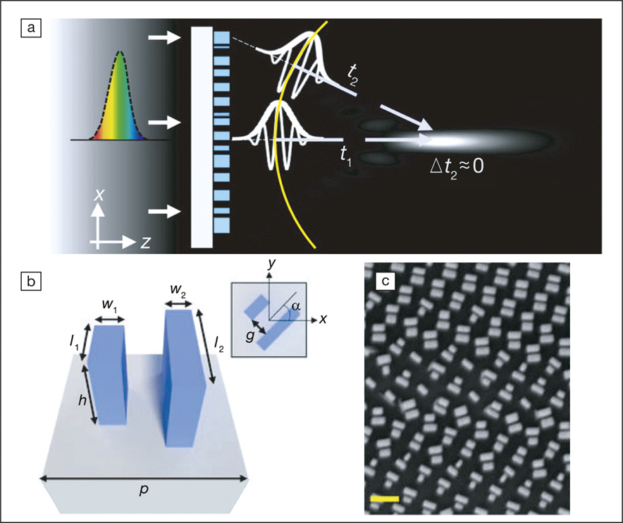
Capasso’s group designed a metalens by assembling pairs of titanium dioxide (TiO2) nanostructures in the form of nanofins on a fused silica substrate. According to first author Wei-Ting Chen, the research group tailored the width, length, and rotation of the two TiO2 rectangles to control both the light’s speed through the assembly, and its exit angle. “At each [metalens] location, there’s a different requirement,” Chen says. Specific TiO2 pairs were placed at precise locations on the substrate to create the desired focusing condition.

(a) Schematic of an achromatic metalens. (b) Schematic of a metalens element. The element consists of one or more TiO2 nanofins of varying dimensions but equal height h = 600 nm, evenly spaced by a distance p = 400 nm. The gap between the nanofins is g = 60 nm. The length l, width w, height h, and rotation angle α are also shown; the subscripts denote the left and right nanofin, respectively. The nanofins are rotated with respect to the center of the square (400 × 400 nm2). (c) Scanning electron micrograph of a region of a fabricated metalens. Scale bar 500 nm. Credit: Nature Nanotechnology.
This metalens design strategy is particularly remarkable for its versatility. “The paper shows an interesting way to manipulate chromatic aberration: you can reduce it, but you can also increase it,” says Arka Majumdar of the University of Washington, who was not connected with this study.
Chen and his colleagues also simulated a metasurface that could be applied to the back of a generic lens. This simulation showed that, with the addition of a specific metasurface, the chromatic aberrations of the simple lens could be corrected and its focusing abilities improved.
“The same design approach can be applied to design optical components for many systems,” Chen says. The Capasso group is interested in applying this approach to make optical components for microscopy, bioimaging systems, and lithography. For applications beyond the visible spectrum, the size of the TiO2 nanostructures could be increased to control light in the infrared region of the spectrum.
This work suggests that big things may be ahead for metasurfaces. Combining this design approach with an optimization algorithm could be used to improve metalens efficiency. According to Majumdar, “An inverse design algorithm could be employed, using optimization techniques to create the metasurface.” To create a desired optical component, a researcher would need to specify the desired functionality to the computer. Then, through numerical optimization, the computer would design the entire metalens to the specification, maximizing its performance. At the moment, the combination of this design approach with such algorithms requires a significant increase in computational power beyond current capabilities. Even so, Majumdar sees this work as “the tip of the iceberg” for future metasurfaces.

