Hostname: page-component-78c5997874-ndw9j Total loading time: 0 Render date: 2024-11-10T06:19:56.397Z Has data issue: false hasContentIssue false

Hard-switching reliability studies of 1200 V vertical GaN PiN diodes

Published online by Cambridge University Press:  28 September 2018
O. Slobodyan
Affiliation:
Sandia National Laboratories, Albuquerque, NM 87185, USA
T. Smith
Affiliation:
Sandia National Laboratories, Albuquerque, NM 87185, USA
J. Flicker
Affiliation:
Sandia National Laboratories, Albuquerque, NM 87185, USA
S. Sandoval
Affiliation:
Sandia National Laboratories, Albuquerque, NM 87185, USA University of Arkansas, Fayetteville, AR 72701, USA
C. Matthews
Affiliation:
Sandia National Laboratories, Albuquerque, NM 87185, USA University of Arkansas, Fayetteville, AR 72701, USA
M. van Heukelom
Affiliation:
Sandia National Laboratories, Albuquerque, NM 87185, USA
R. Kaplar*
Affiliation:
Sandia National Laboratories, Albuquerque, NM 87185, USA
S. Atcitty
Affiliation:
Sandia National Laboratories, Albuquerque, NM 87185, USA
*
Address all correspondence to R. Kaplar at rjkapla@sandia.gov
Get access

Abstract

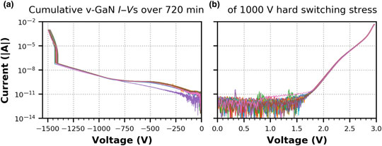
We report on reliability testing of vertical GaN (v-GaN) devices under continuous switching conditions of 500, 750, and 1000 V. Using a modified double-pulse test circuit, we evaluate 1200 V-rated v-GaN PiN diodes fabricated by Avogy. Forward current–voltage characteristics do not change over the stress period. Under the reverse bias, the devices exhibit an initial rise in leakage current, followed by a slower rate of increase with further stress. The leakage recovers after a day's relaxation which suggests that trapping of carriers in deep states is responsible. Overall, we found the devices to be robust over the range of conditions tested.

Type
Research Letters
Copyright
Copyright © Materials Research Society 2018 

Access options

Get access to the full version of this content by using one of the access options below. (Log in options will check for institutional or personal access. Content may require purchase if you do not have access.)

References

1.Millan, J., Godignon, P., Perpina, X., Perez-Tomas, A., and Rebollo, J.: A survey of wide bandgap power semiconductor devices. IEEE Trans. Power Electron. 29, 2155 (2014).10.1109/TPEL.2013.2268900Google Scholar
2.Tsao, J.Y., Chowdhury, S., Hollis, M.A., Jena, D., Johnson, N.M., Jones, K.A., Kaplar, R.J., Rajan, S., Van de Walle, C.G., Bellotti, E., Chua, C.L., Collazo, R., Coltrin, M.E., Cooper, J.A., Evans, K.R., Graham, S., Grotjohn, T.A., Heller, E.R., Higashiwaki, M., Islam, M.S., Juodawlkis, P.W., Khan, M.A., Koehler, A.D., Leach, J.H., Mishra, U.K., Nemanich, R.J., Pilawa-Podgurski, R.C.N., Shealy, J.B., Sitar, Z., Tadjer, M.J., Witulski, A.F., Wraback, M., and Simmons, J.A.: Ultrawide-bandgap semiconductors: research opportunities and challenges. Adv. Electron. Mater. 4, 1600501 (2018).10.1002/aelm.201600501Google Scholar
3.Hudgins, J.L., Simin, G.S., Santi, E., and Khan, M.A.: An assessment of wide bandgap semiconductors for power devices. IEEE Trans. Power Electron. 18, 907 (2003).10.1109/TPEL.2003.810840Google Scholar
4.Baliga, B.J.: Fundamentals of Power Semiconductor Devices (Springer Sciences, New York, 2008).10.1007/978-0-387-47314-7Google Scholar
5.Dickerson, J.R., Allerman, A.A., Bryant, B.N., Fischer, A.J., King, M.P., Moseley, M.W., Armstrong, A.M., Kaplar, R.J., Kizilyalli, I.C., Aktas, O., and Wierer, J.J.: Vertical GaN power diodes with a bilayer edge termination. IEEE Trans. Electron Devices 63, 419 (2016).10.1109/TED.2015.2502186Google Scholar
6.Jones, E.A., Wang, F.F., and Costinett, D.: Review of commercial GaN power devices and GaN-based converter design challenges. IEEE J. Emerging Sel. Topics Power Electron. 4, 707 (2016).10.1109/JESTPE.2016.2582685Google Scholar
7.Kizilyalli, I.C., Edwards, A.P., Nie, H., Disney, D., and Bour, D.: High voltage vertical GaN p–n diodes with avalanche capability. IEEE Trans. Electron Devices 60, 3067 (2013)10.1109/TED.2013.2266664Google Scholar
8.Kizilyalli, I.C., Edwards, A.P., Nie, H., Bour, D., Prunty, T., and Disney, D.: 3.7 kV vertical GaN PN diodes. IEEE Electron Device Lett. 35, 247 (2014).10.1109/LED.2013.2294175Google Scholar
9.Nie, H., Diduck, Q., Alvarez, B., Edwards, A.P., Kayes, B.M., Zhang, M., Ye, G., Prunty, T., Bour, D., and Kizilyalli, I.C.: 1.5-kV and 2.2-m(ohm)-cm2 vertical GaN transistors on bulk-GaN substrates. IEEE Electron Device Lett. 35, 939 (2014).10.1109/LED.2014.2339197Google Scholar
10.Ohta, H., Kaneda, N., Horikiri, F., Narita, Y., Yoshida, T., Mishima, T., and Nakamura, T.: Vertical GaN p–n junction diodes with high breakdown voltages over 4 kV. IEEE Electron Device Lett. 36, 1180 (2015).10.1109/LED.2015.2478907Google Scholar
11.Hu, Z., Nomoto, K., Song, B., Zhu, M., Qi, M., Pan, M., Gao, X., Protasenko, V., Jena, D., and Xing, H.G.: Near unity ideality factor and Shockley-read-hall lifetime in GaN-on-GaN p–n diodes with avalanche breakdown. Appl. Phys. Lett. 107, 243501 (2015).10.1063/1.4937436Google Scholar
12.del Alamo, J.A. and Joh, J.: GaN HEMT reliability. Microelectron. Reliab. 49, 1200 (2009).10.1016/j.microrel.2009.07.003Google Scholar
13.King, M.P., Dickerson, J.R., DasGupta, S., Marinella, M.J., Kaplar, R.J., Piedra, D., Sun, M., and Palacios, T.: Trapping characteristics and parametric shifts in lateral GaN HEMTs with SiO2/AlGaN gate stacks, in Reliability Physics Symposium (IRPS), 2015 IEEE Proceedings, Monterey, CA, USA, 2015, Start Page: IEEE. doi: 10.1109/IRPS.2015.7112689.Google Scholar
14.Wu, Y., Chen, C.Y., and del Alamo:, J.A. Electrical and structural degradation of GaN high electron mobility transistors under high-power and high-temperature direct current stress. J. Appl. Phys. 117, 025707 (2015).10.1063/1.4905677Google Scholar
15.Bahl, S.R., Kim, J., Fu, L., Sasikumar, A., Chatterjee, T., and Pendrakhar, S.: Application reliability validation of GaN power devices, presented at the Electron Devices Meeting (IEDM), 2016 IEEE International, San Francisco, CA, USA, 2016, doi: 10.1109/IEDM.2016.7838461.Google Scholar
16.Kizilyalli, I.C., Bui-Quang, P., Disney, D., Bhatia, H., and Aktas, O.: Reliability studies of vertical GaN devices based on bulk GaN substrates. Microelectron. Reliab. 55, 1654 (2015).10.1016/j.microrel.2015.07.012Google Scholar
17.Slobodyan, O., Sandoval, S., Flicker, J., Kaplar, R.J., Matthews, C., van Heukelom, M., and Atcitty, S.: Switching reliability characterization of vertical GaN PiN diodes, presented at the Electrical Energy Storage Applications and Technology, 2017, San Diego, CA, USA, 2017.Google Scholar
18.Kizilyalli, I.C., Edwards, A.P., Aktas, O., Prunty, T., and Bour, D.: Vertical power p–n diodes based on bulk GaN. IEEE Trans. Electron Devices 62, 414 (2015).10.1109/TED.2014.2360861Google Scholar
19.Matthews, C., Flicker, J., Kaplar, R.J., van Heukelom, M., Atcitty, S., Kizilyalli, I.C., and Aktas, O.: Switching characterization of vertical GaN PiN diodes, presented at the Wide Bandgap Power Devices and Applications (WiPDA), 2016 IEEE 4th Workshop, Fayetteville, AR, USA, 2016, doi: 10.1109/WiPDA.2016.7799924.Google Scholar
Supplementary material: File

Slobodyan et al. supplementary material

Slobodyan et al. supplementary material 1

Download Slobodyan et al. supplementary material(File)
File 2.4 MB