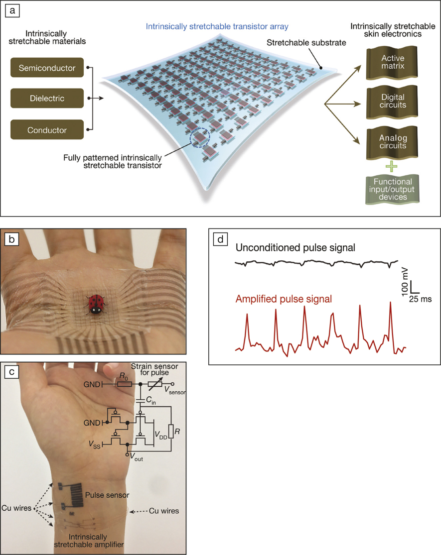
The field of bioelectronics is rapidly growing, and lightweight sensors that could be utilized in the pedantic monitoring of human health are becoming the next big thing. Now a team of researchers from Stanford University, Samsung Advanced Institute of Technology, and Gyeongsang National University has developed a scalable fabrication process to create a stretchable transistor array that could be attached to skin to monitor health, as reported in a recent issue of Nature (doi:10.1038/nature25494).
This research utilizes an intrinsically stretchable and semiconducting polymer to create a transistor array that can be used as a sensor for pulse rate monitoring. “The stretchable amplifier circuits built up by these transistors could also be utilized for the measurement of other physiological signals, including ECG, EMG, body temperature, sweat, etc.,” says Sihong Wang from Stanford University, who is a lead author in this study. Although inorganic materials dominate the field of transistors, their rigid nature makes them undesirable for medical applications. “Through using electronic materials with intrinsic stretchability to build such electronics, we can concurrently achieve high transistor density and high mechanical stretchability, thus providing the practical feasibility to realize advanced functionalities with long-term biomechanical robustness,” Wang says.
The transistor device density of 347 transistors per square centimeter is achieved with a charge-carrier mobility (0.98 cm2 V–1 s–1) that is comparable to amorphous silicon, and which is maintained when these devices are subjected to 100% strain for 1000 cycles. Additionally, the stretchable transistor array devices show ideal switching behavior, with no current hysteresis, minimal gate leakage, and good stability (shelf and under bias) making it viable in electronic applications. Its ability to be operated at low voltages (∼10 V) enables it to be employed for on-skin applications.
Developing these polymer-based sensors is tricky as the standard photolithographic microfabrication procedure concomitantly creates a damaging environment for the polymers. The novel fabrication process starts with the silicon wafer, which is coated with dextran. This sacrificial layer is water soluble and enables the final separation. The stretchable dielectric is deposited and photo-patterned on the dextran-coated silicon wafer. A semiconductor and conductor deposition and patterning follow the dielectric deposition to create the source/drain electrodes of the transistor. The stretchable substrate is laminated, and water is used to remove the sacrificial layer, which detaches the polymers from the silicon wafer. The final fabrication step involves the deposition and patterning of gate electrodes. The newly developed fabrication processes can be scaled up to produce 6300 transistors over an area of 4.4 × 4.4 cm2. This is the earliest demonstration of skin-like stretchable circuits, maintaining its properties, as the basic components of skin electronics.

(a) Three-dimensional diagram of an intrinsically stretchable transistor array as the core building block of skin electronics. (b) A tactile sensor array made from a stretchable active matrix adheres and conforms to a human palm, enabling accurate sensing of the position of a synthetic ladybug with six conductive legs. (c) Use of the intrinsically stretchable amplifier to amplify arterial pulse signals measured by a stretchable strain sensor. The devices are attached on skin side-by-side. Electrical connections are made using Cu wires (as marked) attached on the contacting pads by anisotropic conductive tapes. The inset shows the circuit diagram. (d) Pulse signals obtained, before and after amplification, using the same scale. Credit: Sihong Wang.
Sahika Inal of King Abdullah University of Science and Technology (KAUST) appreciates this study. “This work overcomes the current engineering challenges in fabricating a flexible and stretchable, polymer-based electronic circuitry comprising multiple functional electronic components. As such, the device is the closest that the organic electronics get to the performance rigid silicon circuits despite its impressive mechanical properties,” Inal says.


