Introduction
The mechanism of spatial electromagnetic (EM) wave protection is usually to control properties of the free space propagating EM waves, including amplitude, frequency, energy, etc. This can be achieved by using structural artificial EM materials, such as frequency selective surfaces (FSS) [Reference Munk1] or EM metamaterials [Reference Capolino2]. In recent years, with the increasing complexity of the EM environment and the upgrading of electronic countermeasure level, EM stealth [Reference Wang, Chen, Li and Cao3–Reference Choudhary, Pal and Sarkhel5] and high-power microwaves (HPM) protection [Reference Katko, Hawkes, Barrett and Cummer6–Reference Zhao, Wang and Aditya8] have become two research focus in the design of EM structures, for which the researchers have proposed frequency selective rasorber (FSR, such as in papers [Reference Bakshi, Mitra and Teixeira9–Reference Wang, Min, Zhao, Yuan, Li, Hu and Cao12]) and energy selective surface (ESS, such as in papers [Reference Zhou and Shen13–Reference Zhou and Shen15]).
The FSR was initially proposed for the application in radome that requires not only wave absorbing for stealth but also transmitting for communication purposes. The two functions usually lie in different frequency bands. Recent studies in this field mainly focus on performance improvement or reconfigurability [Reference Bakshi, Mitra and Teixeira9–Reference Chen, Lu, Liu and Jiang11]. The ESS, on the other hand, was proposed to protect electronic devices from the HPM in the transmission band. Recent studies to achieve energy selection focus on using self-actuated protection structures. This field is becoming a research hotspot while many problems remain in real applications [Reference Zhou and Shen13–Reference Zhou and Shen15].
As discussed, both techniques were proposed to protect electronic devices but in different frequency bands and with different mechanisms. Although researchers have conducted much research in both fields, reports on the integration design of these two techniques are rarely seen.
In response to the actual demand for integrated stealth and energy protection for electronic equipment in the complex EM environment, an energy selective rasorber (ESR) that combines the technique of ESS and FSR is proposed that has the function of both energy selective protection in the communication band (0.8–2 GHz) and wave absorbing in the stopping band (6–18 GHz), as illustrated in Fig. 1(a). The design is finally proved by theoretical analysis, simulation optimization, and prototype measurement.
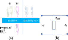
Figure 1. (a) Responses of the proposed energy selective absorber under different incident powers ![]() ${P_1},$
${P_1},$ ![]() ${P_2}$ in different frequency bands. (b) Equivalent two-port network model to describe an ESS.
${P_2}$ in different frequency bands. (b) Equivalent two-port network model to describe an ESS.
Theoretical analysis to achieve energy selective absorber (ESA) functions
An FSR can be considered an ordinary FSS for which the stopping band is designed to absorb EM waves for the stealth requirement. Thus, the design of an FSR can be commonly achieved using the traditional FSS design technique coupled with the frequency selective absorber (FSA) technique. The next step is to include energy selectivity into the passband, for which a brief theoretical analysis is given here to describe the primary mechanism.
The mechanism to achieve an ESS by using diodes and the FSS technique has already been discussed in [Reference Katko, Hawkes, Barrett and Cummer6, Reference Zhao, Wang and Aditya8], for which the response differences to incident power levels are mainly caused by the nonlinear diodes’ different on/off states. According to requirements, the responses of an ESS to different incident EM waves can be described in Fig. 1(a), in which the transmission or reflection states are decided by the different incident power levels ![]() ${P_1}$ and
${P_1}$ and ![]() ${P_2}$ (usually
${P_2}$ (usually ![]() ${P_2}$ stands for HPM; thus
${P_2}$ stands for HPM; thus ![]() ${P_2} \gg {P_1}$). The ESS is modeled as an equivalent transmission line to analyze the mechanism theoretically, as shown in Fig. 1(b). During the design, the two ports are in matching conditions, then one can obtain the transmission coefficient as
${P_2} \gg {P_1}$). The ESS is modeled as an equivalent transmission line to analyze the mechanism theoretically, as shown in Fig. 1(b). During the design, the two ports are in matching conditions, then one can obtain the transmission coefficient as
 \begin{equation}{S_{21}} = {2 \over {2 + {Z_0}/{Z_{{\textrm{ESS}}}}}}\end{equation}
where ![]() ${Z_0}$ and
${Z_0}$ and ![]() ${Z_{{\textrm{ESS}}}}$ are the impedances of the air and the ESS, as illustrated in the figure. Considering the function requirements of an ESS, the transmission coefficient should be adaptively adjusted to the power level of the incident EM waves. For example, when it requires high transmittance (high
${Z_{{\textrm{ESS}}}}$ are the impedances of the air and the ESS, as illustrated in the figure. Considering the function requirements of an ESS, the transmission coefficient should be adaptively adjusted to the power level of the incident EM waves. For example, when it requires high transmittance (high ![]() ${S_{21}}$) for low-power incidence, then
${S_{21}}$) for low-power incidence, then ![]() ${Z_{{\textrm{ESS}}}}$ is needed to be large; when it requires shielding effect for high-power incidence, then
${Z_{{\textrm{ESS}}}}$ is needed to be large; when it requires shielding effect for high-power incidence, then ![]() ${Z_{{\textrm{ESS}}}}$ is needed to be small. Although the opposite requirements (transmittance for high-power incidence, shielding for low power) are rarely published, a similar mechanism can also be applied.
${Z_{{\textrm{ESS}}}}$ is needed to be small. Although the opposite requirements (transmittance for high-power incidence, shielding for low power) are rarely published, a similar mechanism can also be applied.
Based on this analysis, the mechanism of an ESS is to achieve an impedance shift caused by the incident EM power. This can be directly done using active components such as PIN diodes, which are also the most commonly used components for current ESS designs, such as in papers [Reference Zhou and Shen13–Reference Zhou and Shen15].
The relation between incident power and reflectance is a continuous process, as shown in Fig. 2. This is rarely mentioned in previous ESS studies because phases P1 and P3 are mainly focused on providing enough transmission and reflection. However, because the diodes applied for the ESS study are not ideal components, the unavoidable phase P2 should be noticed and usually needs to be minimized through careful design.
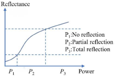
Figure 2. Relation between incident power and reflectance for a typical ESS.
After designing an ESS that satisfies a given requirement, it is necessary to couple the ESS into the FSR design. The direct idea is to replace the bottom layer of the FSR with the designed ESS with a similar structure, thus minimizing the effect on the absorbing function. However, the introduction of the commonly used active devices directly affects the performance of the absorbing band. Therefore, integration design and parameter optimization are required.
Structure design
Based on the previous design principles, this section investigates the structure design to achieve specific functions. As discussed, we design an absorbing structure and then change the bottom layer structure into a passband ESS structure. Because the coupling among the different functional layers significantly affects the whole performance, parameter adjustment and component model optimization are done to optimize the design.
Design of the absorbing structure
To start, a structure with a wide absorbing band of 6–18 GHz and a low passband of 0.8–2 GHz is designed. A classical double square loop metal structure with lumped resistors is used here as the initial unit cell to achieve a strong absorption outside the passband. The two loops in the structure are coupled to produce multiple resonant effects, thus presenting strong induced currents to absorb EM waves in the required absorbing band. In the passband, however, there should be no resonances. Therefore, no absorption occurs to guarantee the transmission of EM waves.
Based on the analysis, Fig. 3 shows the designed absorbing structure, which consists of a resistive layer, a supporting dielectric layer, an air layer, and a metal plate. The commonly used equivalent circuit model/method (ECM) [Reference Munk1] is applied here to explain the performance of the design. Figure 3(c) presents the ECM for the absorbing structure, in which the capacitors come from gaps in the structure, and inductors come from metal strips. The two routes a and b stand for the two square loops. ![]() ${L_p}$ stands for the combination of the dielectric layer, the air gap, and the metal ground. It is clear from the ECM that double resonances can be obtained while the absorbing property is achieved by adjusting resistors
${L_p}$ stands for the combination of the dielectric layer, the air gap, and the metal ground. It is clear from the ECM that double resonances can be obtained while the absorbing property is achieved by adjusting resistors ![]() ${R_{\textrm{a}}}$,
${R_{\textrm{a}}}$, ![]() ${R_{\textrm{b}}}$ and the value of
${R_{\textrm{b}}}$ and the value of ![]() ${L_p}$.
${L_p}$.
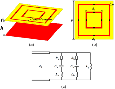
Figure 3. (a) 3D view and (b) top view of the absorbing unit, (c) ECM of the structure. The red parts stand for the metal strips, the yellow for the dielectric support, and the black for the resistors.
The initial parameters of the structure (such as periodicity and loop length) are set according to the FSS design principle [Reference Munk1]. Then, the initial parameters are optimized to obtain the best performance. Finally, the periodicity of the unit is set as ![]() $p = 13.5$ mm. The edge length of the outer loop is
$p = 13.5$ mm. The edge length of the outer loop is ![]() ${d_1} = 11.2$ mm, and the inner loop is
${d_1} = 11.2$ mm, and the inner loop is ![]() ${d_2} = 5.8$ mm. The width of the square loop is
${d_2} = 5.8$ mm. The width of the square loop is ![]() $w = 0.4$ mm. The resistance value of the outer loop is
$w = 0.4$ mm. The resistance value of the outer loop is ![]() $300$ Ω and the inner loop
$300$ Ω and the inner loop ![]() $120$ Ω. The resistors are placed at the center of each inner and outer loop edge. The material of the dielectric layer is F4BM220 (
$120$ Ω. The resistors are placed at the center of each inner and outer loop edge. The material of the dielectric layer is F4BM220 (![]() ${\varepsilon _{\textrm{r}}} = 2.2$) with a thickness of
${\varepsilon _{\textrm{r}}} = 2.2$) with a thickness of ![]() $t = 0.25$ mm. The height of the air layer is
$t = 0.25$ mm. The height of the air layer is ![]() $h = 5$ mm.
$h = 5$ mm.
The broadband absorbing performance for the structure is affected by the matching property between the surface impedance and the free-space impedance, which is mainly determined by the distance ![]() $h$ between the resistive surface and the lower metal plate, and the resistance value of the resistors on the square loop. The reflection coefficient S 11 of the structure under different values of
$h$ between the resistive surface and the lower metal plate, and the resistance value of the resistors on the square loop. The reflection coefficient S 11 of the structure under different values of ![]() $h$ are shown in Fig. 4. As can be seen, when
$h$ are shown in Fig. 4. As can be seen, when ![]() $h = 5$ mm (this value is also chosen for fabrication cost considerations), the S 11 in 6–18 GHz is less than −10 dB, thus satisfying the requirement.
$h = 5$ mm (this value is also chosen for fabrication cost considerations), the S 11 in 6–18 GHz is less than −10 dB, thus satisfying the requirement.
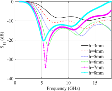
Figure 4. Reflection coefficients versus frequency under different values of ![]() $h$.
$h$.
Design of the ESS layer
To introduce a power protection function in the transmission band into the absorber, the bottom metal plate was redesigned to achieve a transmission band with an energy-selective function. Since the reform of the lower layer structure affects the total absorber, optimization needs to be done after an ESS layer is designed to substitute the bottom layer. In this work, the ESS layer is designed to function in 0.8–2 GHz while there should not be any high harmonics or gate flaps in the whole working band of 0.8–18 GHz. Otherwise, the absorption effect will be affected.
Based on the analysis, the bottom ESS layer is designed as shown in Fig. 5, where two metal strips are detached from the metal plate, leaving a thin metal strip in the middle. Then, this metal strip’s middle part (1.2 mm in length) is replaced with a Schottky diode of HSMS-2864. Similarly, the structure is supported by an F4BM220 (![]() ${\varepsilon _{\textrm{r}}} = 2.2$) dielectric plate with thickness
${\varepsilon _{\textrm{r}}} = 2.2$) dielectric plate with thickness ![]() $t = 0.25$ mm. In a unit structure, the metal strip width
$t = 0.25$ mm. In a unit structure, the metal strip width ![]() ${W_1} = 1.5$ mm and width
${W_1} = 1.5$ mm and width ![]() ${W_2} = 1$ mm. Figure 5(b) presents the ECM of the ESS layer, in which the components are all generated using similar methods as in Fig. 3(c). Notice that the introduction of the passband brings an additional contribution of
${W_2} = 1$ mm. Figure 5(b) presents the ECM of the ESS layer, in which the components are all generated using similar methods as in Fig. 3(c). Notice that the introduction of the passband brings an additional contribution of ![]() ${Z_0}$ from free space, and both a capacitor and a diode are introduced to describe the performance of the real diode (the actual ECM of a diode should include a series inductor, a parallel capacitor, and an ideal diode. Here, the effect of inductance is included in
${Z_0}$ from free space, and both a capacitor and a diode are introduced to describe the performance of the real diode (the actual ECM of a diode should include a series inductor, a parallel capacitor, and an ideal diode. Here, the effect of inductance is included in ![]() ${L_e}$).
${L_e}$).
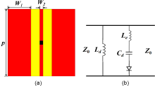
Figure 5. Structure of the bottom ESS layer (a) and its ECM (b). The red parts stand for the metal strips, the yellow for the dielectric support, and the black for the diode.
The transmission and reflection coefficient (in the form of S parameters) curves under low-power incidence in 0.8–18 GHz are shown in Fig. 6, which is obtained by field and circuit co-simulation. To explain the behavior under low-power incident conditions, considering on the ESS layer, there exists a parasitic capacitance and an inductance near 17 GHz due to the package of the diode, of the values around 0.5pF and 0.5nH.
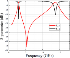
Figure 6. Co-simulation results under low-power EM incidence.
From Fig. 6, the existence of the resonance affects the absorption rate in 6–18 GHz. Thus, optimizing the structure parameters is necessary to eliminate the influence of parasitic inductance on the absorption band. An iterative parameter optimization procedure should be done because this adjustment also affects the transmission property in the low-frequency range.
To minimize the resonance in the high-frequency range, two packages of diodes are used in parallel to substitute the single one, resulting in equivalence to the parallel connection of a parasitic inductance and a parasitic capacitance, thus can reduce the inductance and increase the capacitance, as shown in Fig. 7(a). It can be seen that the reduction of the high resonance leads to a better wide-band absorbing performance in 6–18 GHz. The final structure is shown in Fig. 7(b), where the metal strip width ![]() ${W_1} = {W_2} = 1.5$ mm and the gap width
${W_1} = {W_2} = 1.5$ mm and the gap width ![]() $g$ = 1.4 mm (the gap is lengthened to facilitate the loading of diodes).
$g$ = 1.4 mm (the gap is lengthened to facilitate the loading of diodes).
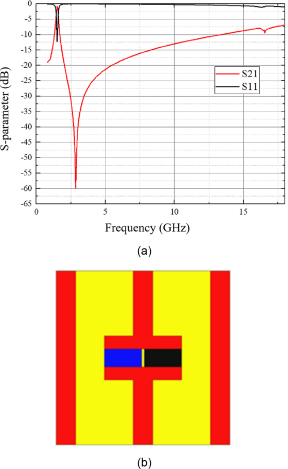
Figure 7. (a) Co-simulation results under low-power EM incidence for the modified design and (b) unit structure of the modified design. The red parts stand for the metal strips, the yellow for the dielectric support, and the black and blue for the two diodes packages.
Design of the whole structure
Direct substituting the previously designed ESS layer to the bottom layer of the absorber will lead to an impedance mismatch, thus degrading the whole performance. Here, optimization is done by adjusting the height ![]() $h$ of the air layer and the length of the inner and outer loops on the top layer. Notice that the ECM analysis of the whole structure is not a necessary step because the derivation of the entire ECM is straightforward by simply connecting the previous two ECMs. At the same time, the resulting complex ECM is troublesome to calculate and loses its instructive property.
$h$ of the air layer and the length of the inner and outer loops on the top layer. Notice that the ECM analysis of the whole structure is not a necessary step because the derivation of the entire ECM is straightforward by simply connecting the previous two ECMs. At the same time, the resulting complex ECM is troublesome to calculate and loses its instructive property.
The final obtained transmission and reflection coefficients are shown in Fig. 8, in which both results under low- (14 dBm) and high-power (30dBm) incidences are included. As can be seen, under low-power incidence (solid red and black lines), both the S 11 and S21 parameters are less than −10 dB, which means it has high absorption in 6–18 GHz. While in the designed transmission band, the peak S 21 value is greater than −2 dB in 0.8–2 GHz, which can guarantee efficient transmission. Under high-power incidence (dotted red and black lines), similar absorption results are obtained in 6–18 GHz, while in the transmission band, incident EM waves are blocked as S 21 is less than −15 dB. Parameters for the final design are ![]() $h = 4$ mm,
$h = 4$ mm, ![]() ${d_1} = 11$ mm,
${d_1} = 11$ mm, ![]() ${d_2} = 5.2$ mm.
${d_2} = 5.2$ mm.
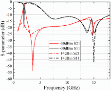
Figure 8. Simulation results for the integrated structure.
Fabrication and measurement
Fabrication and measurement are needed to verify the performance of the multifunctional design. This work uses two different measurement methods—the waveguide method for energy selective property and the free-space method for absorbing property—for measurement. Therefore, two measurement samples of different sizes are fabricated. The effectiveness of the waveguide method for energy selection measurement has been proved in many previous works [Reference Zhou and Shen13–Reference Zhou and Shen15].
The measurement sample for verifying the energy selection property using the waveguide method is shown in Fig. 9, in which the waveguide measurement system is also shown. The sample size was fabricated as ![]() $161.1\;{\rm{mm}} \times 106.4\;{\textrm{mm}}$ to facilitate the aperture size of the waveguide, which contains
$161.1\;{\rm{mm}} \times 106.4\;{\textrm{mm}}$ to facilitate the aperture size of the waveguide, which contains ![]() $4 \times 8$ unit cells. A polymethacrylimide foam separates the two dielectric plates in the structure, for which the EM parameters are equivalent to the air. In the upper layer, chip resistors in package 0402 are used; in the bottom layer, the Schottky diode in the HSMS-2864 package is used.
$4 \times 8$ unit cells. A polymethacrylimide foam separates the two dielectric plates in the structure, for which the EM parameters are equivalent to the air. In the upper layer, chip resistors in package 0402 are used; in the bottom layer, the Schottky diode in the HSMS-2864 package is used.
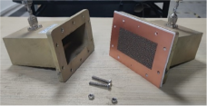
Figure 9. Fabricated sample and the waveguide measurement system.
Measurement results under different power incidences are shown in Fig. 10. It can be seen that at 1.86 GHz, when the incident power changes from −30 to 14 dBm, the S 11 parameter changes from below −22 dB to above −2 dB, while the S 21 parameter changes from above −2 dB to below −17 dB. Detailed comparisons of simulated and measured peak frequencies/amplitudes are shown in Table 1. It can be seen that the measured results agree well with the simulations, thus proving the effectiveness of the energy selectivity.
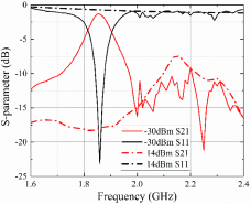
Figure 10. Measured result using waveguide measurement method.
Table 1. Comparison of simulation and measurement results

Next, a sample of ![]() $27\;{\rm{cm}} \times 27\;{\rm{cm}}$ (containing
$27\;{\rm{cm}} \times 27\;{\rm{cm}}$ (containing ![]() $19 \times 19$ unit cells) is fabricated for the free-space measurement, as shown in Fig. 11, where the left and right subfigures stand for the front and bottom views. The sample is measured in an anechoic chamber, and the results are shown in Fig. 12. Notice that there is a frequency shift between simulation and measurement (around 14 GHz), possibly caused by fabrication error or the inaccuracy of the active component model. This frequency shift also leads to the value differences between simulation and measurement. However, this does not upset the final results because both the variation trends and average values are much the same. It can also be seen that both the measured S 11 and S 21 parameters have an average value below −10 dB in 6–18 GHz (except for a slight exceed around 17 GHz for measurement, which is due to the measurement errors), which proves the design to have a good absorption effect.
$19 \times 19$ unit cells) is fabricated for the free-space measurement, as shown in Fig. 11, where the left and right subfigures stand for the front and bottom views. The sample is measured in an anechoic chamber, and the results are shown in Fig. 12. Notice that there is a frequency shift between simulation and measurement (around 14 GHz), possibly caused by fabrication error or the inaccuracy of the active component model. This frequency shift also leads to the value differences between simulation and measurement. However, this does not upset the final results because both the variation trends and average values are much the same. It can also be seen that both the measured S 11 and S 21 parameters have an average value below −10 dB in 6–18 GHz (except for a slight exceed around 17 GHz for measurement, which is due to the measurement errors), which proves the design to have a good absorption effect.
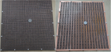
Figure 11. Fabricated sample for free space measurement.
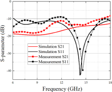
Figure 12. Measured results using the free space measurement method.
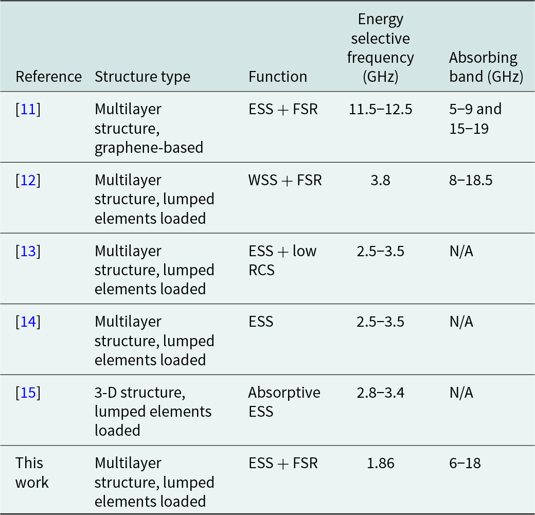
To compare this work with recently published similar works, Table 2 is given to further describe the advantages of this design. As can be seen, this work combines both energy selectivity and wave absorption simultaneously, while only lumped elements are used (unlike in paper [Reference Chen, Lu, Liu and Jiang11], graphene is introduced). At the same time, the absorbing band is much improved.
Table 2. Comparison of recent similar works
Conclusion
This work proposes a multifunction structural artificial EM material that has the functions of an energy-selective transmission around 1.86 GHz and a wideband wave-absorbing in the 6–18 GHz. The design can protect not only electronic devices from wideband radar detections but also from interference, such as HPM in the communication band.
Although the integration design achieves the required functions, many improvements remain, such as angular stability or polarization insensitivity. Notice that these problems for each function structure can be solved using previously reported methods. However, after integration, some of these problems become serious that should be further studied.
Funding
This work was supported by the Natural Science Foundation of China under project number 61871219; the open research fund of the State Key Laboratory of Millimeter Waves under project number K202324.
Competing interests
The authors report no conflict of interest.

Kun Yan is currently pursuing the Ph.D. degree with the College of Automation Engineering, Nanjing University of Aeronautics and Astronautics. Her current research interests include aircraft overall design, modeling, simulation (especially of the electromagnetic field) modeling and target detection technology.

Yi Wang received his Ph.D. at Nanjing University of Aeronautics and Astronautics in 2012, where he has been working and became a full-time university associate professor in 2015. He worked as a visiting scholar at Purdue University for a year in 2018. He has authored more than 100 research articles. His current research interests include the theory and design of artificial electromagnetic (EM) materials and computational electromagnetics and EM simulation.

Xiaofan Min received his master’s degree at Nanjing University of Aeronautics and Astronautics in 2023. He is currently working in the field of microwave components and system design.

Lei Tang is a graduate student pursuing his master’s degree at the Nanjing University of Aeronautics and Astronautics. He is currently working in the field of artificial electromagnetic materials, especially the design of energy selective surfaces.

Yu Xia received his master’s degree at the Nanjing University of Aeronautics and Astronautics in 2022. He is currently working in the field of microwave components and system design.

You Li received his Ph.D. at the Nanjing University of Aeronautics and Astronautics in 2021. He is currently working at Nanjing Electronic Equipment Institute, and his research interests focus on the design and application of artificial electromagnetic materials.


