Researchers from Oak Ridge National Laboratory’s Institute for Functional Imaging of Materials (ORNL-IFIM) have succeeded in training a neural network to identify different two-dimensional (2D) lattices and defects in scanning transmission electron microscope (STEM) images. This work, directed by Sergei Kalinin and published recently in ACS Nano (doi:10.1021/acsnano.7b07504), is an important step toward the creation of autonomous microscopes that can image and identify samples in real time.
Neural networks are automated computerized systems that perform data-intensive tasks with greater complexity. In self-driving cars, neural networks are trained to distinguish between the road and obstacles, such as potholes or pedestrians. To operate safely on the road, a self-driving car must be constantly collecting and analyzing information from its surroundings.
In a material, understanding fundamental microstructural characteristics, such as lattice defects, requires analysis of many images from electron and scanning probe microscopy. The ubiquity of STEM, atomic force microscopy, and similar instruments in laboratories has led to facile generation of large sets of data for materials characterization. “Nowadays, the amount of data obtained in a single experiment is so large that manual analysis requires an unreasonable amount of time,” says Maxim Ziatdinov, a postdoctoral candidate at IFIM and first author of the article.
To address this problem, Kalinin’s research team designed a neural network that could accurately classify defects in 2D materials. Researchers simulated basic lattice structures and simple defects using density functional theory (DFT). The simulated images formed a set of “classes” that the network then compared to experimental STEM images. The network analyzes the differences between the simplistic simulated classes and the experimental images and incorporates these differences into classes of increasing complexity. According to Ziatdinov, “The neural network is able to learn [the] ‘concept’ of what the atomic lattice is and how defects look in general in a way, similar to a human student learning these concepts.”

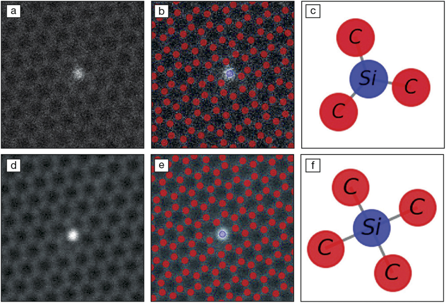
From analysis of pixels in an image to the analysis of single defects in graphene using a neural network. (a) Experimental image of a threefold coordinated silicon defect. (b) Result of the neural network automated analysis of (a). (c) Graphical representation of single defect structure for the threefold silicon defect. (d–f) Same as (a–c) for fourfold coordinated silicon defect. Imaging area: 1.95 nm × 1.95 nm (a, d). Credit: ACS Nano.
The theoretical image set used to train the neural network included images that corresponded to a hexagonal lattice, similar to a graphene lattice, and two types of defects. The neural network then learned how to identify increasingly complicated defects, for example, differentiating between silicon defects that were bonded to three versus four carbons in a graphene sheet.
From there, the researchers demonstrated that the network can be generalized to more complex 2D lattices, such as tungsten-doped molybdenum disulfide. Here again, the neural network was able to identify many different types of defects, accurately identifying locations in the lattice when one versus two selenide atoms were absent. According to Juan Carrasquilla, a researcher at the Vector Institute for Artificial Intelligence, “This shows the generalization power of their model and the broad applicability of the authors’ ideas.” Carrasquilla was not involved with this study.
The ORNL-IFIM researchers see many future applications for neural networks in materials science characterization. By changing the initial training sets but not the architecture of the neural network itself, the network can learn to identify different materials and lattice structures. Ziatdinov hopes to create a “universal deep learning model that will allow analyzing any material with any type of lattice,” potentially even in three dimensions.
“This work paves the way toward automatization of the analysis of experimental data available with modern microscopy,” Carrasquilla says. This could lead to autonomous microscopes, which can take and analyze images of a sample simultaneously. “This process can be automated, dramatically speeding the identification of defects in functional materials and the understanding needed to engineer next-generation nanoscale materials and devices,” Kalinin says.


