


Introduction
Rat-race couplers (RRCs) are crucial components in communication systems. They are extensively utilized in a variety of microwave circuits, such as balanced power amplifiers, phase shifters, data modulators, and mixers. Many studies have focused on improving some features of the RRCs, such as enhanced bandpass characteristics [Reference Gruszczynski and Wincza1–Reference Ahn and Tentzeris3], reduced size [Reference Tseng and Chang4, Reference Tolin, Bahr and Vipiana5], harmonic suppression [Reference Jianzhong and Xiaowei6, Reference Nie, Luo, Guo and Fan7], and a high power division ratio [Reference Park and Lee8, Reference Chaudhary and Jeong9]. Otherwise, to improve the performance of the system in terms of high capacity, multi-task, and compact size, it requires that the system can operate with different frequencies. Hence, the requirement for the design of multi-band components has become more and more essential. The RRCs were investigated to work in multi-band, such as dual-band, tri-band, and quad-band. To design the dual-band RRCs, the researchers have introduced several structures including Pi-shaped configurations [Reference Chi and Ho10, Reference Tseng, Mou, Lin and Chao11], T-shaped structures [Reference Zhang and Chen12, Reference Majeed and Ashraf13], step-impedance sections [Reference Chin, Lin, Wei, Tseng and Yang14], and synthetic transmission lines [Reference Chen, Sim and Wu15] to replace quarter-wavelength transmission lines in the conventional RRCs. Tri-band RRCs were designed using various techniques. In [Reference Zhebin and Park16], a tri-band Pi-shaped structure incorporating resonators was proposed, while [Reference Chu and Lin17] employed a T-shaped step-impedance transformer to achieve tri-band performance. Notably, three operating frequencies in the work [Reference Chu and Lin17] are not completely independent since the middle frequency is an average of the upper and lower frequencies. Another method is the application of metamaterial in [Reference Cheng and Ming18], but this type causes complexity in analysis and fabrication.
In recent years, with the advancement of quad-band applications, various quad-band circuits have been studied, such as quad-band filters [Reference Wei, Zhang, Yue and Shi19, Reference Wei, Yue, Zhang and Shi20], quad-band antennas [Reference Abdalla and Hu21, Reference Maamria, Challal, Benmahmoud, Fertas and Mesloub22], and quad-band power amplifiers [Reference Keshavarz, Mohammadi and Abdipour23]. However, research on quad-band RRCs remains limited. To the best of the author’s knowledge, only studies [Reference Althuwayb24], [Reference Papanastasiou25], and [Reference Velan, Kingsly, Kanagasabai, Alsath, Panneer and Subbaraj26] have addressed these issues so far. In [Reference Althuwayb24], a quad-band RRC was designed using a Pi-shaped quad-band microstrip line. However, its frequency ratio of the largest to the smallest operating frequency is restricted to 4.5, as shown in [Reference Giang, Thang, Manh and Huong27], where the same quad-band structure was used in a Wilkinson power divider. Since both designs are based on replacing the 70.71-ohm quarter-wavelength transmission line with the same Pi-shaped quad-band structure, they share the same frequency ratio limitation, making them less suitable for wideband applications. The study in [Reference Papanastasiou25] introduced a quad-band RRC designed with negative-refractive-index transmission lines and incorporating MIM capacitors and chip inductors. However, the quad-band RRC [Reference Papanastasiou25] exhibits limitations in terms of low isolation and poor insertion loss. A quad-band RRC with spurious pass-band suppression was introduced in [Reference Velan, Kingsly, Kanagasabai, Alsath, Panneer and Subbaraj26]. This design used a laterally offset dual ring (LODR) resonator backed with concentric dual split ring (CDSR) slots. It is observed that this quad-band RRChas the disadvantages of a high insertion loss and significant phase deviation. Thus, some problems obtained in the previous quad-band RRCs need to be solved to achieve high performance.
This paper presents a novel and simple design of a quad-band RRC based on a proposed modified T-shaped structure (MTSS). Two coupled lines are integrated into the conventional dual-band T-shaped structure to form the MTSS. The MTSS are then employed to replace the quarter-wavelength transmission lines in the conventional RRC. Compared to previously reported quad-band RRCs [Reference Papanastasiou25, Reference Velan, Kingsly, Kanagasabai, Alsath, Panneer and Subbaraj26], which rely on negative refractive index transmission lines with lumped components [Reference Papanastasiou25] or complex two-layer structures [Reference Velan, Kingsly, Kanagasabai, Alsath, Panneer and Subbaraj26], the proposed quad-band RRC employs a simpler design approach. It features a planar structure without any lumped elements. The closed-form design equations for the proposed structure are derived through analytical methods. Moreover, a detailed analysis of the design constraints is provided, demonstrating that the proposed quad-band RRC can achieve a frequency ratio between the highest and lowest operating frequencies not exceeding 5.39. To evaluate the effectiveness of the design method, a prototype of quad-band RRC operating at 0.6, 1.196, 1.853, and 2.45 GHz was designed, fabricated, and tested. Good agreement between the simulation and measurement results validates the feasibility of the proposed approach. The measured results show that at the four operating frequencies, the proposed quad-band RRC exhibits an insertion loss of less than 4.4 dB, while simultaneously achieving a return loss exceeding 21.75 dB and an isolation level greater than 21.6 dB.
Model and formulation of the proposed MTSS
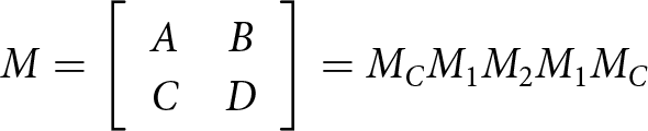
The proposed MTSS is presented in Fig. 1(b). This MTSS is equivalent to a quarter-wavelength transmission line with a characteristic impedance of  ${Z_T}$ (Fig. 1a) at four operating bands. The proposed MTSS is developed by adding two series coupled lines to the conventional dual-band T-shaped structure [Reference Sahu, Shamaileh, Aaen and Abu-shamleh28]. The MTSS is composed of two transmission lines, two coupled lines, and a short stub. Two transmission lines are the same with characteristic impedance ${Z_1}$ and electrical length $\theta $. Two coupled lines have the same even and odd characteristic impedances ( ${Z_e}$ and ${Z_o}$) and the same electrical length $\theta $. The short stub has characteristic impedance ${Z_2}$ and electrical length $\theta $.
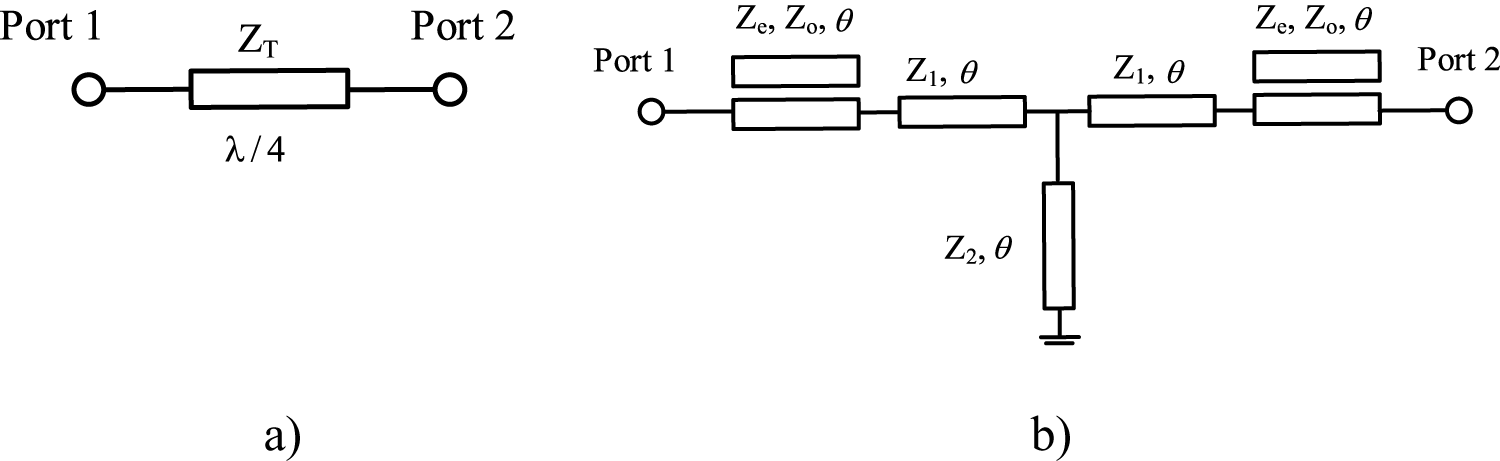
Figure 1. (a) A quarter-wavelength transmission line. (b) A proposed modified T-shape structure.
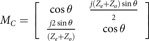
To determine the parameters of the proposed MTSS, the methodology from [Reference Althuwayb24] was applied. The ABCD matrix of the proposed MTSS is the product of ABCD matrices of sections:
 \begin{equation}M = \left[ {\begin{array}{*{20}{c}}
A&B \\
C&D
\end{array}} \right] = {M_C}{M_1}{M_2}{M_1}{M_C}\end{equation}
\begin{equation}M = \left[ {\begin{array}{*{20}{c}}
A&B \\
C&D
\end{array}} \right] = {M_C}{M_1}{M_2}{M_1}{M_C}\end{equation} In which,  ${M_C}$, ${M_1}$, and ${M_2}$ are ABCD matrices of coupled line, transmission line ( ${Z_1}$, $\theta $), and short stub ( ${Z_2}$, $\theta $), respectively. These matrices are determined as follows:
 \begin{equation}{M_C} = \left[ {\begin{array}{*{20}{c}}
{\cos \theta }&{\frac{{j({Z_e} + {Z_o})\sin \theta }}{2}} \\
{\frac{{j2\sin \theta }}{{({Z_e} + {Z_o})}}}&{\cos \theta }
\end{array}} \right]\end{equation}
\begin{equation}{M_C} = \left[ {\begin{array}{*{20}{c}}
{\cos \theta }&{\frac{{j({Z_e} + {Z_o})\sin \theta }}{2}} \\
{\frac{{j2\sin \theta }}{{({Z_e} + {Z_o})}}}&{\cos \theta }
\end{array}} \right]\end{equation}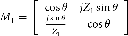 \begin{equation}{M_1} = \left[ {\begin{array}{*{20}{c}}
{\cos \theta }&{j{Z_1}\sin \theta } \\
{\frac{{j\sin \theta }}{{{Z_1}}}}&{\cos \theta }
\end{array}} \right]\end{equation}
\begin{equation}{M_1} = \left[ {\begin{array}{*{20}{c}}
{\cos \theta }&{j{Z_1}\sin \theta } \\
{\frac{{j\sin \theta }}{{{Z_1}}}}&{\cos \theta }
\end{array}} \right]\end{equation}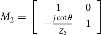 \begin{equation}{M_2} = \left[ {\begin{array}{*{20}{c}}
1&0 \\
{ - \frac{{j\cot \theta }}{{{Z_2}}}}&1
\end{array}} \right]\end{equation}
\begin{equation}{M_2} = \left[ {\begin{array}{*{20}{c}}
1&0 \\
{ - \frac{{j\cot \theta }}{{{Z_2}}}}&1
\end{array}} \right]\end{equation} Besides, the ABCD matrix of the quarter-wavelength transmission line with characteristics impedance  ${Z_T}$ has the following form:
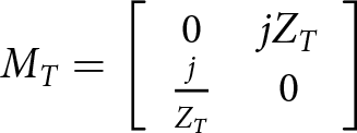 \begin{equation}{M_T} = \left[ {\begin{array}{*{20}{c}}
0&{j{Z_T}} \\
{\frac{j}{{{Z_T}}}}&0
\end{array}} \right]\end{equation}
\begin{equation}{M_T} = \left[ {\begin{array}{*{20}{c}}
0&{j{Z_T}} \\
{\frac{j}{{{Z_T}}}}&0
\end{array}} \right]\end{equation}To make the proposed MTSS equivalent to the quarter-wavelength transmission line, the following relation must be satisfied:
 \begin{equation}{M_C}{M_1}{M_2}{M_1}{M_C} = \pm {M_T}\end{equation}
Hence,
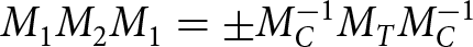 \begin{equation}{M_1}{M_2}{M_1} = \pm M_C^{ - 1}{M_T}M_C^{ - 1}\end{equation}
By substituting Equations (2)–(4) and (5) into Equation (7), the following equation is obtained:
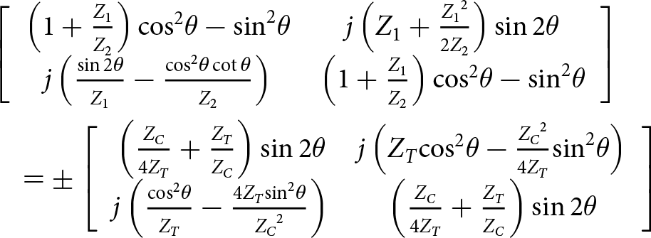 \begin{align}
&\left[ {\begin{array}{*{20}{c}}
{\left( {1 + \frac{{{Z_1}}}{{{Z_2}}}} \right){{\cos }^2}\theta - {{\sin }^2}\theta }&{j\left( {{Z_1} + \frac{{{Z_1}^2}}{{2{Z_2}}}} \right)\sin 2\theta } \\
{j\left( {\frac{{\sin 2\theta }}{{{Z_1}}} - \frac{{{{\cos }^2}\theta \cot \theta }}{{{Z_2}}}} \right)}&{\left( {1 + \frac{{{Z_1}}}{{{Z_2}}}} \right){{\cos }^2}\theta - {{\sin }^2}\theta }
\end{array}} \right] \nonumber \\
& \quad = \pm \left[ {\begin{array}{*{20}{c}}
{\left( {\frac{{{Z_C}}}{{4{Z_T}}} + \frac{{{Z_T}}}{{{Z_C}}}} \right)\sin 2\theta }&{j\left( {{Z_T}{{\cos }^2}\theta - \frac{{{Z_C}^2}}{{4{Z_T}}}{{\sin }^2}\theta } \right)} \\
{j\left( {\frac{{{{\cos }^2}\theta }}{{{Z_T}}} - \frac{{4{Z_T}{{\sin }^2}\theta }}{{{Z_C}^2}}} \right)}&{\left( {\frac{{{Z_C}}}{{4{Z_T}}} + \frac{{{Z_T}}}{{{Z_C}}}} \right)\sin 2\theta }
\end{array}} \right] \end{align}
\begin{align}
&\left[ {\begin{array}{*{20}{c}}
{\left( {1 + \frac{{{Z_1}}}{{{Z_2}}}} \right){{\cos }^2}\theta - {{\sin }^2}\theta }&{j\left( {{Z_1} + \frac{{{Z_1}^2}}{{2{Z_2}}}} \right)\sin 2\theta } \\
{j\left( {\frac{{\sin 2\theta }}{{{Z_1}}} - \frac{{{{\cos }^2}\theta \cot \theta }}{{{Z_2}}}} \right)}&{\left( {1 + \frac{{{Z_1}}}{{{Z_2}}}} \right){{\cos }^2}\theta - {{\sin }^2}\theta }
\end{array}} \right] \nonumber \\
& \quad = \pm \left[ {\begin{array}{*{20}{c}}
{\left( {\frac{{{Z_C}}}{{4{Z_T}}} + \frac{{{Z_T}}}{{{Z_C}}}} \right)\sin 2\theta }&{j\left( {{Z_T}{{\cos }^2}\theta - \frac{{{Z_C}^2}}{{4{Z_T}}}{{\sin }^2}\theta } \right)} \\
{j\left( {\frac{{{{\cos }^2}\theta }}{{{Z_T}}} - \frac{{4{Z_T}{{\sin }^2}\theta }}{{{Z_C}^2}}} \right)}&{\left( {\frac{{{Z_C}}}{{4{Z_T}}} + \frac{{{Z_T}}}{{{Z_C}}}} \right)\sin 2\theta }
\end{array}} \right] \end{align} In Equation (8), we set  ${Z_C} = {Z_e} + {Z_o}$. By solving Equation (8), the following relations are deduced:
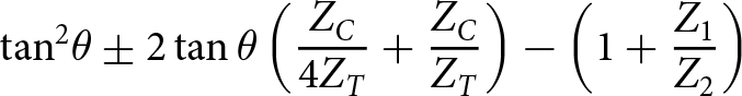 \begin{equation}{\tan ^2}\theta \pm 2\tan \theta \left( {\frac{{{Z_C}}}{{4{Z_T}}} + \frac{{{Z_C}}}{{{Z_T}}}} \right) - \left( {1 + \frac{{{Z_1}}}{{{Z_2}}}} \right)\end{equation}
 \begin{equation}{\tan ^2}\theta \pm 2\tan \theta \left( {{Z_1} + \frac{{{Z^2}_1}}{{2{Z_2}}}} \right)\frac{{4{Z_T}}}{{Z_C^2}} - \frac{{4{Z^2}_T}}{{Z_C^2}}\end{equation}
For the MTSS to operate at four bands, the system of Equations (9) and (10) must have four distinct solutions, namely θ 1, θ 2, θ 3, and θ 4. These represent the electrical lengths corresponding to the four operating frequencies f 1, f 2, f 3, and f 4. Consequently, Equation (9) must be identical to Equation (10), meaning their coefficients must be equal. From this condition, the following equations are obtained:
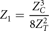 \begin{equation}{Z_1} = \frac{{Z_C^3}}{{8Z_T^2}}\end{equation}
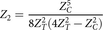 \begin{equation}{Z_2} = \frac{{Z_C^5}}{{8Z_T^2(4Z_T^2 - Z_C^2)}}\end{equation}
 \begin{equation}\tan \theta = \pm \sqrt {\frac{{4Z_T^2}}{{Z_C^2}} + \frac{{{{\left( {Z_C^2 + 4Z_T^2} \right)}^2}}}{{16Z_T^2Z_C^2}}} \pm \frac{{Z_C^2 + 4Z_T^2}}{{4{Z_T}{Z_C}}}\end{equation}
From Equation (13), we deduce:
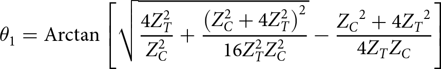 \begin{equation}{\theta _1} = {\text{Arctan}}\left[ {\sqrt {\frac{{4Z_T^2}}{{Z_C^2}} + \frac{{{{\left( {Z_C^2 + 4Z_T^2} \right)}^2}}}{{16Z_T^2Z_C^2}}} - \frac{{{Z_C}^2 + 4{Z_T}^2}}{{4{Z_T}{Z_C}}}} \right]\end{equation}
 \begin{equation}{\theta _2} = {\text{Arctan}}\left[ {\sqrt {\frac{{4Z_T^2}}{{Z_C^2}} + \frac{{{{\left( {Z_C^2 + 4Z_T^2} \right)}^2}}}{{16Z_T^2Z_C^2}}} + \frac{{{Z_C}^2 + 4{Z_T}^2}}{{4{Z_T}{Z_C}}}} \right]\end{equation}
 \begin{equation}{\theta _3} = \pi - {\theta _2}\end{equation}
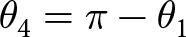 \begin{equation}{\theta _4} = \pi - {\theta _1}\end{equation}
From Equations (16) and (17), the following relations are obtained:
 \begin{equation}\frac{{{f_2}}}{{{f_1}}} = \frac{{{\theta _2}}}{{{\theta _1}}}\end{equation}
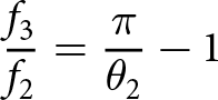 \begin{equation}\frac{{{f_3}}}{{{f_2}}} = \frac{\pi }{{{\theta _2}}} - 1\end{equation}
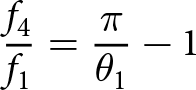 \begin{equation}\frac{{{f_4}}}{{{f_1}}} = \frac{\pi }{{{\theta _1}}} - 1\end{equation}
Thus, based on the derived equations, MTSS can be designed.
Next, we present an illustrative example of designing an impedance-matching circuit between 75 $\Omega $ and 100 $\Omega $ at four frequency bands, utilizing the proposed MTSS. It assumed that the first and final frequencies are ${f_1} = 1{\text{ GHz}}$ and ${f_4} = 4{\text{ }}$GHz, respectively. The process of design includes the following steps. First of all, we calculate the characteristic impedance ${Z_T}$ of the quarter-wavelength transmission line for matching between $75{ \Omega }$ and $100{ \Omega }$, ${Z_T} = \sqrt {75.100} = 86.6{ \Omega }$. Next, the quarter-wavelength transmission line ${Z_T}$ is replaced by the proposed MTSS. Parameters of the proposed MTSS are calculated by applying the closed-form equations (11)–(20). ${\theta _1}$ is determined by using Equation (20), ${\theta _1} = {36^o}$. By substituting ${\theta _1}$ and ${Z_T}$ to Equation (14), ${Z_C}$ is given as $120{ \Omega }$. By using Equations (15) and (18), we obtain ${f_2}$ = 1.965 GHz. From Equation (19), ${f_3}$ is calculated as 3.035 GHz. Impedances ${Z_1}$ and ${Z_2}$ are determined from Equation (11) and (12), ${Z_1} = 28.8{ \Omega }$, ${Z_2} = 26.6{ \Omega }$.
Finally, the impedance matching circuit is simulated to verify the calculation method. Figures 2 and 3 illustrate the ideal simulated parameters |S 11|, |S 22|, and |S 21| of the circuit.
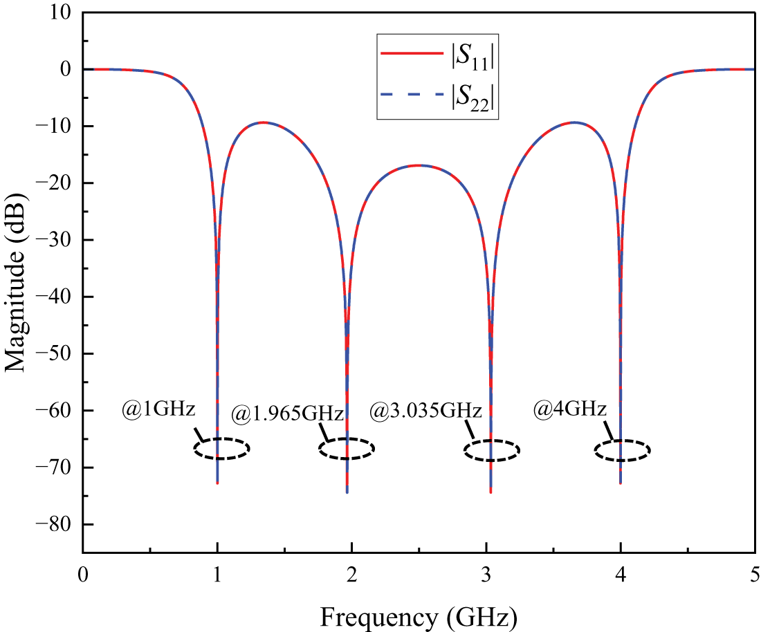
Figure 2. The ideal simulated scattering parameters |S 11| and |S 22| of the impedance matching circuit between 75  $\Omega $ and 100 $\Omega $.
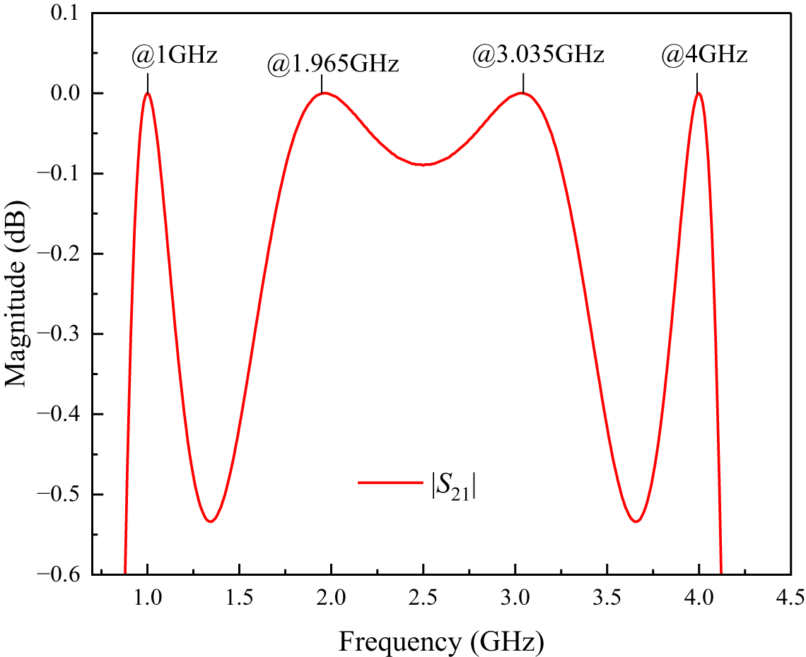
Figure 3. The ideal simulated scattering parameter |S 21| of the impedance matching circuit between 75  $\Omega $ and 100 $\Omega $.
In Fig. 2, it can be observed that the reflection coefficients ∣S 11∣ and ∣S 22∣ exhibit identical responses and reach their minimum points at the four designed frequencies 1, 1.965, 3.035, and 4, with values lower than −53 dB. Additionally, Fig. 3 shows that the transmission coefficient ∣S 21∣ approaches its maximum value of 0 dB at these four design frequencies. These results indicate that the impedance-matching circuit performs effectively, confirming the validity of the design method. The following section will present the design approach for a quad-band RRC based on the proposed MTSS.
Design method of quad-band RRC
The conventional single-band RRC is presented in Fig. 4 [Reference Pozar29].
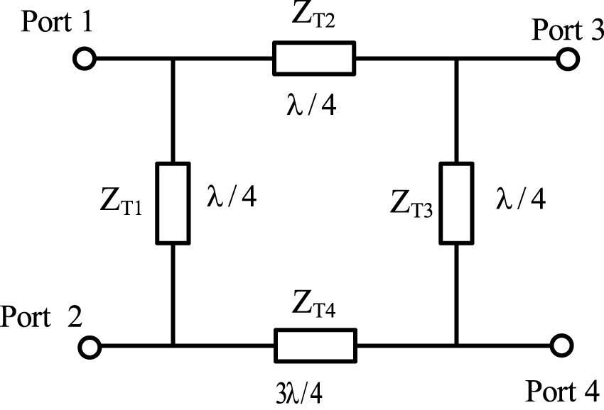
Figure 4. The conventional single-band rat-race coupler [Reference Pozar29].
Figure 4 illustrates a conventional single-band RRC, in which transmission lines are connected to form a circular or square ring. The RRC consists of four ports, including input, output, coupled, and isolated ports. In the RRC, three transmission lines with characteristic impedances  ${Z_{T1}},{\text{ }}{Z_{T2}}$, and ${Z_{T3}}$ are quarter-wavelength (λ/4) lines, and one transmission line with characteristics impedance ${Z_{T4}}$ is a three-quarter-wavelength (3λ/4) line. All of the transmission lines have the same characteristics as follows:
 \begin{equation}{Z_{T1}} = {Z_{T2}} = {Z_{T3}} = {Z_{T4}} = {Z_T} = {Z_0}\sqrt 2 \Omega\end{equation}
 where  ${Z_0}$= 50 $\Omega $.
A proposed quad-band RRC is depicted in Fig. 5. To design the quad-band RRC, the quarter-wavelength transmission lines  ${Z_{T1}},{\text{ }}{Z_{T2}}$, and ${Z_{T3}}$ in the conventional RRC are replaced by the proposed MTSS blocks, which are, respectively, symbolized as E1, E2, and E3. Since the transmission line ${Z_{T4}}$ has an electrical length of 3λ/4, it is divided into three quarter-wavelength transmission lines with the characteristic impedance ZT 4. Then, these three quarter-wavelength transmission lines are replaced by MTSS blocks E41, E42, and E43.
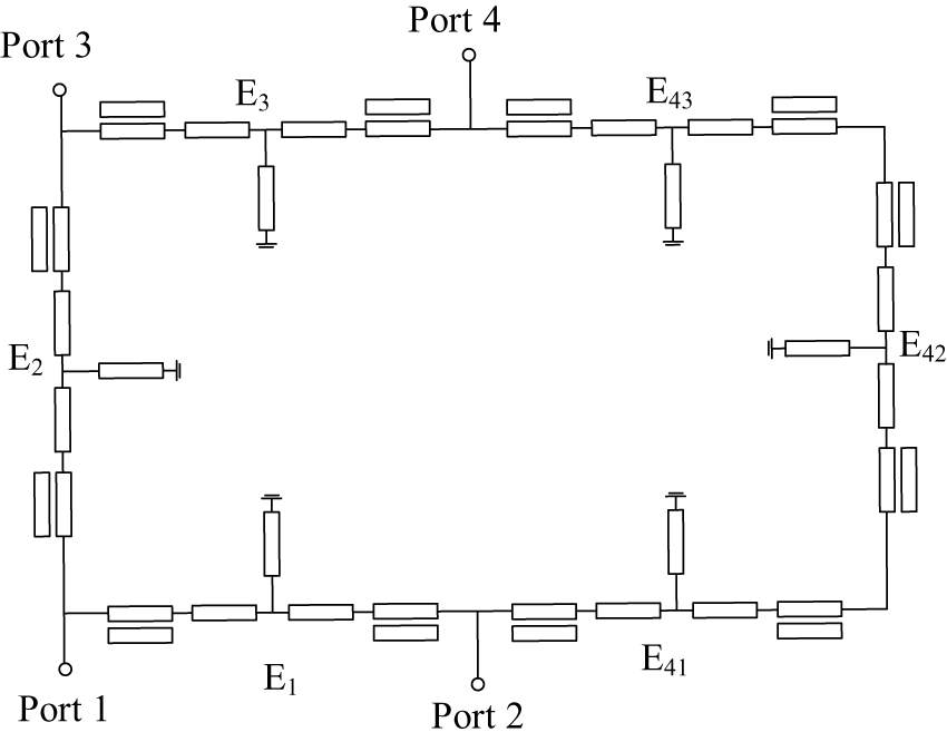
Figure 5. The proposed quad-band RRC.
Next, the design constraints of the proposed quad-band RRC are analyzed. When the characteristic impedance of a transmission line is too high or too low, the line width becomes excessively narrow or wide. A narrow line is challenging to fabricate, whereas a wide line significantly increases transmission loss. Therefore, an important design constraint is related to the standard PCB technology, which requires all characteristic impedances  ${Z_1}$ and ${Z_2}$ of the circuit to be in the range from 15 Ω to 120 Ω. From Equations (11) and (12), the following conditions are deduced:
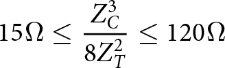 \begin{equation}{15_{}}\Omega \leq \frac{{Z_C^3}}{{8Z_T^2}} \leq {120_{}}\Omega \end{equation}
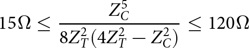 \begin{equation}{15_{}}\Omega \leq \frac{{Z_C^5}}{{8Z_T^2(4Z_T^2 - Z_C^2)}} \leq {120_{}}\Omega \end{equation}
Solving the system of inequalities (22) and (23) with the condition Z T = 70.71, we obtain
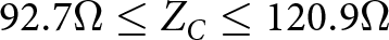 \begin{equation}92.7 \Omega \leq Z_C \leq 120.9 \Omega \end{equation}
By substituting condition (24) into Equations (14) and (15), the following conditions are derived:
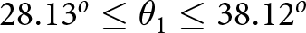 \begin{equation}{28.13^o} \leq {\theta _1} \leq {38.12^o}\end{equation}
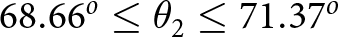 \begin{equation}{68.66^o} \leq {\theta _2} \leq {71.37^o}\end{equation}
By substituting Equation (25) into Equation (20), and Equation (26) into Equation (19), we have
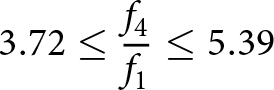 \begin{equation}3.72 \leq \frac{{{f_4}}}{{{f_1}}} \leq 5.39\end{equation}
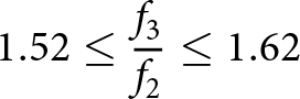 \begin{equation}1.52 \leq \frac{{{f_3}}}{{{f_2}}} \leq 1.62\end{equation}
Thus, from the above analysis, it can be concluded that the proposed quad-band RRC can operate at four operating bands, provided that the condition f 4/f 1 ≤ 5.39 is satisfied. This constraint ensures the feasibility of fabricating the quad-band RRC using conventional PCB technology.
From the design equations presented earlier, it also can be seen that when f 1 and f 4 are selected, the frequencies f 2 and f 3 are also determined based on the values of f 1 and f 4. Next, the dependence of the four fractional bandwidths (FBWs) of the quad-band RRC, namely  ${\Delta }$f 1, ${\Delta }$f 2, ${ \Delta }$f 3, and ${\Delta }$f 4 on the frequency ratio ${\text{ }}{f_4}/{f_1}$, is investigated. The bandwidth is defined as the range where |S 11| is less than −15 dB. Figure 6 illustrates the simulated dependence of these four FBWs on the frequency ratio f 4/f 1 .
From Fig. 6, it can be observed that as the frequency ratio f 4/f 1 increases, the FBW of the first band (Δf 1) exhibits a significant upward trend, indicating a notable expansion in bandwidth. The second band (Δf 2) also shows a moderate increase, though with a much slower rate compared to Δf 1. Meanwhile, the third (Δf 3) and fourth (Δf 4) bands remain nearly constant with minor variations, implying minimal dependence on the frequency ratio f 4/f 1 . These trends highlight the impact of the frequency ratio f 4/f 1 on the four FBWs of the proposed quad-band RRC.
Figure 6. The dependence of four bandwidths of the quad-band RRC on the frequency ratio  ${f_4}/{f_1}$.
Finally, the process of designing a quad-band RRC includes the following steps:
1. Separate the conventional RRC into $\lambda /4$ transmission lines with the same characteristic impedance,
${Z_T} = 70.71{ \Omega }$. The
$3\lambda /4$ transmission line is separated into three
$\lambda /4$ transmission lines.
$\lambda /4$ transmission lines with the same characteristic impedance,
${Z_T} = 70.71{ \Omega }$. The
$3\lambda /4$ transmission line is separated into three
$\lambda /4$ transmission lines.2. Replace the quarter-wavelength transmission lines with equivalent MTSS blocks. Parameters of the MTSS are calculated as below.
2.1. Select the minimum and maximum operating frequencies,
${f_1}$ and
${f_4}$, these frequencies must satisfy the condition (27).2.2. From Equation (20), determine the electrical length
${\theta _1}$.2.3. Substitute
${Z_T}$ and
${\theta _1}$ into Equation (14), then calculate the value of
${Z_C}$.2.4. From Equation (15), determine the value of
${\theta _2}$.2.5. Use Equations (18) and (19) to calculate operation frequencies
${f_2}$ and
${f_3}$.2.6. Determine the characteristic impedances
${Z_1}$ and
${Z_2}$ using Equations (11) and (12).


Experimental validation
For further demonstration, a quad-band RRC was designed, fabricated, and tested. The circuit was fabricated using a Rogers RO4003C substrate, which has a relative dielectric constant of 3.55, a thickness of 0.813 mm, and a loss tangent of 0.0027.
Applying the design procedure presented in the previous section, the parameters of the scheme are calculated. Firstly, we choose frequencies  ${f_4}$ = 2.45 GHz and ${f_1}$ = 0.6 GHz. Then, these frequencies are substituted into Equation (20), and the electrical length ${\theta _1}$ is defined as ${\theta _1}$ = 35.4°. From Equations (14) and (15), the values of ${Z_C}$ and ${\theta _2}$ are computed as ${Z_C}$= 99.6 Ω and ${\theta _2}$= 70.6°. From there, Z e = 51 Ω and Z o = 48.6 Ω are chosen. From Equations (18) and (19), the operating frequencies ${f_2}$ and ${f_3}$ are defined as ${f_2}$ = 1.196 GHz, ${f_3}$ = 1.853 GHz. Substituting the values of ${Z_C}$ and ${Z_T}$ into Equations (11) and (12), we have ${Z_1}$ = 24.7 Ω and ${Z_2}$ = 24.3 Ω. The selected frequency bands 0.6, 1.196, 1.853, and 2.45 GHz correspond to various practical applications: 0.6 GHz for low-frequency wireless communication systems such as LTE Band 71 (600 MHz), which is currently used to provide extended coverage in 4G and 5G networks; 1.196 GHz for global navigation satellite systems (e.g., Galileo E5b, GPS L5); 1.853 GHz for mobile communication; and 2.45 GHz (ISM band) for WLAN and wireless sensor networks. These bands highlight the versatility of the proposed design for modern communication systems.
Figure 7 shows the layout and fabricated prototype of the proposed quad-band RRC. A Vector Network Analyzer is employed to measure the scattering parameters of the fabricated prototype.
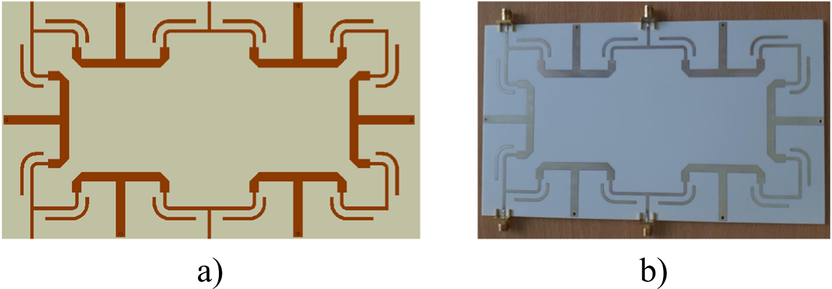
Figure 7. (a) Layout and (b) photograph of the fabricated quad-band RRC.
Simulated and measured performance of the designed quad-band RRC are presented in Figs. 8–11. The performance results demonstrate the presence of four passbands centered at 0.6, 1.195, 1.825, and 2.42 GHz. There is a slight shift in the center frequencies of each band, which becomes more pronounced at higher frequencies. This shift is primarily attributed to transmission line discontinuities, including T-junction and bend discontinuities. Additionally, at higher frequencies, the shorter wavelength increases the model’s sensitivity to etching inaccuracies, which can affect overall performance. Nevertheless, within the considered frequency range, the proposed model exhibits reliable performance, as validated by both simulation and experimental results. The results suggest that impedance mismatches caused by additional junctions in the proposed circuit have a limited impact within the studied range. However, this behavior may vary if the operating frequency range is extended, and further investigation is required to fully assess the impact under such conditions.
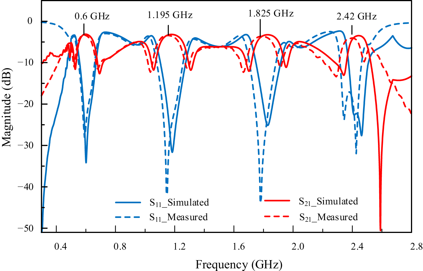
Figure 8. Measured and simulated parameters S 21 and S 11 of the proposed quad-band RRC.
Figure 8 shows that the measured insertion losses |S 21| at the four operating frequencies 0.6, 1.195, 1.825, and 2.42 GHz are 3.18, 3.03, 3.14, and 3.53 dB, respectively. Thus, compared to the ideal 3 dB level, the additional insertion loss is less than 0.53 dB. Meanwhile, the measured input return loss |S 11| is better than 21.75 dB at all four central operating frequencies.
Figure 9 describes the measured and simulated |S 31| and |S 41| parameters of the proposed quad-band RRC. The simulated and measured results show a close agreement. From the graph of Fig. 9, the measured insertion loss |S 31| at four operating bands is lower than 4.4 dB. Meanwhile, the measured isolation level (|S 41|) is higher than 21.6 dB.
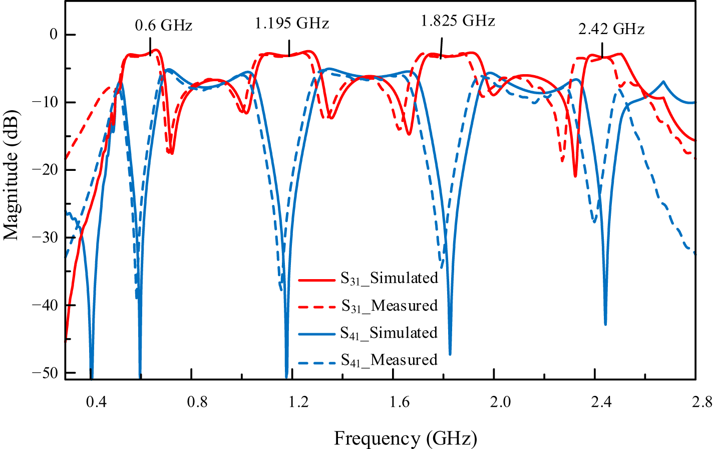
Figure 9. Measured and simulated parameters S 31 and S 41 of the proposed quad-band RRC.
In-phase response of the proposed quad-band RRC is depicted in Fig. 10. The detailed data indicate that at the four operating frequencies 0.6, 1.195, 1.825, and 2.42 GHz, the phase differences  $\angle {S_{21}} - \angle {S_{31}}$ are 3.45o, 4.56o, 2.58o, and 1.3o, respectively. Figure 11 illustrates the out-phase responses $\angle {S_{24}} - \angle {S_{34}}$ of the RRC. The results show that at four operating frequencies, the phase differences are within 180o ± 6.7o.
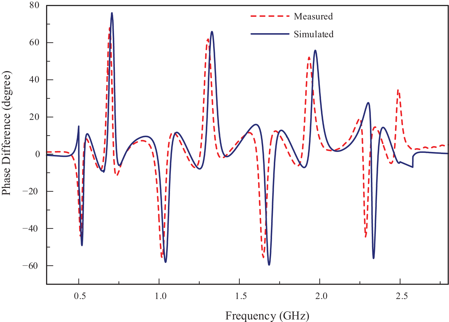
Figure 10. Simulated and measured phase difference between S 21 and S 31 of the proposed quad-band RRC.
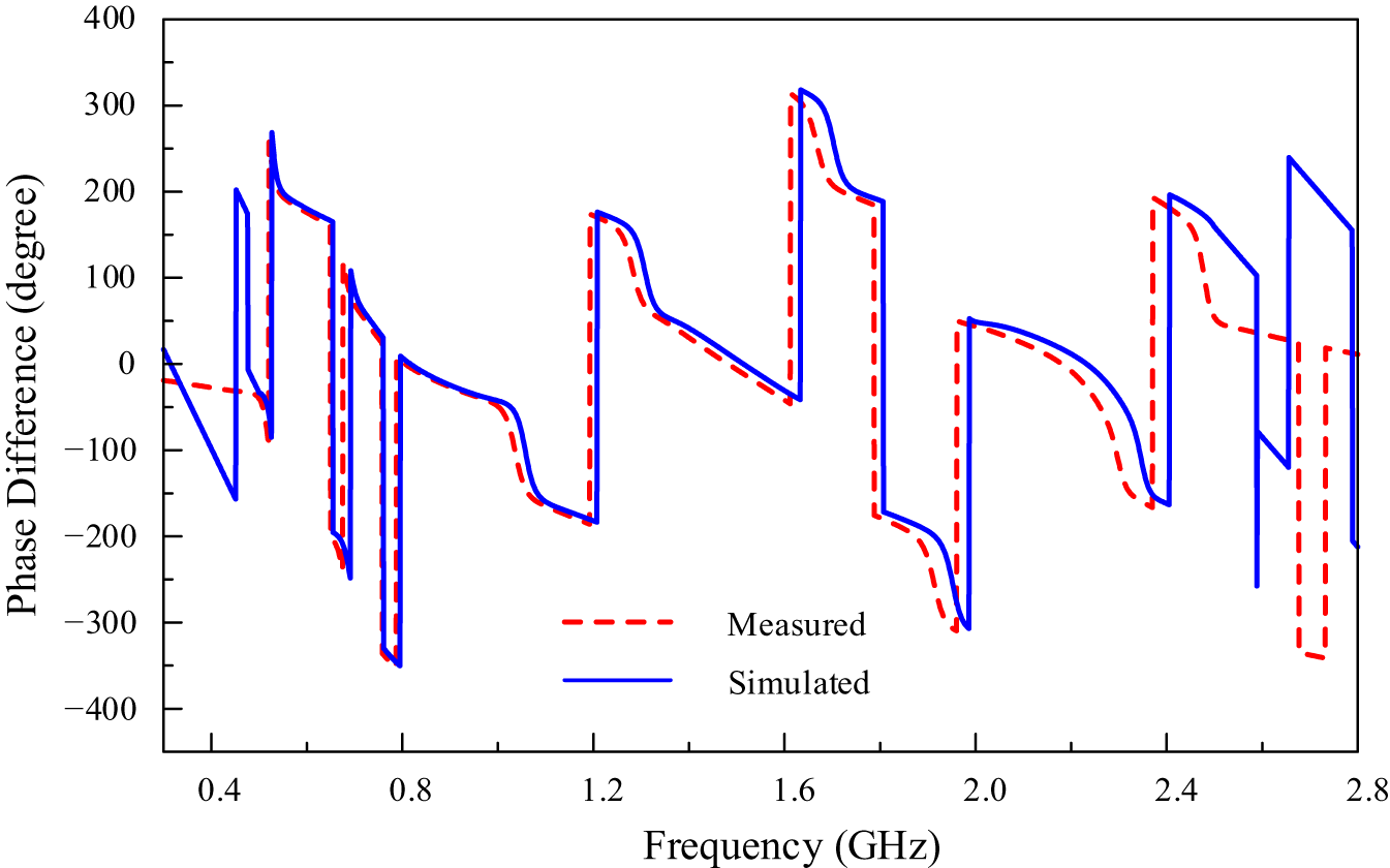
Figure 11. Simulated and measured phase difference between S 24 and S 34 of the proposed quad-band RRC.
Finally, to evaluate the effectiveness of the design approach, the measured performance of the proposed quad-band RRC is compared with other reported works. Comparison results are listed in Table 1.
Table 1. Comparison performance of the proposed quad-band RRC and other reported works

In Table 1, NI indicates no information; PD is the phase difference; IRL, IS, and IL denote input return loss, isolation, and insertion loss at the four operating frequencies, respectively; BLC is the branch line coupler; λg is the guided wavelength at frequency f 1; and FBW is the fractional bandwidth. The FBW is defined as the frequency range where the amplitude imbalance between the two output ports remains within 1 dB for both the proposed quad-band RRC and [Reference Piazzon, Saad, Colantonio, Giannini, Andersson and Fager30], whereas for [Reference Guoan, Shihao, Wenguang, Baoquan and Lamin31], it is within 1 dB for the first two bands and 1.5 dB for the last two bands.
Compared to the previously published works [Reference Papanastasiou25, Reference Piazzon, Saad, Colantonio, Giannini, Andersson and Fager30–Reference Liang, Zhang and Liao32], the proposed quad-band RRC exhibits a significant improvement in isolation, return loss, and insertion loss performance. Specifically, it achieves an isolation level exceeding 21.6 dB, return losses greater than 21.75 dB, and an insertion loss of less than 4.4 dB at four operating frequencies. Although the circuit in [Reference Velan, Kingsly, Kanagasabai, Alsath, Panneer and Subbaraj26] achieves better isolation, it exhibits a high insertion loss of up to 6.3 dB and significant phase deviation. Moreover, the proposed RRC design is simpler than those presented in [Reference Papanastasiou25, Reference Velan, Kingsly, Kanagasabai, Alsath, Panneer and Subbaraj26], as it features a planar structure, does not use lumped elements, and relies solely on coupled lines, transmission lines, and short stubs. Meanwhile, the quad-band RRC in [Reference Papanastasiou25] utilizes negative refractive index transmission lines with MIM capacitors and inductors, while the circuit in [Reference Velan, Kingsly, Kanagasabai, Alsath, Panneer and Subbaraj26] employs a laterally offset dual-ring (LODR) resonator backed by concentric dual-split-ring (CDSR) slots and is implemented in a two-layer structure. Thus, these comparisons validate the advantages of the proposed design method. However, despite these benefits, the proposed circuit also presents some drawbacks. The main drawback is its relatively large size compared to the circuits listed in Table 1. This size increase represents a trade-off for achieving a simpler structure and improved performance. In addition, the use of multiple cascaded λ/4 transmission line sections introduces another potential limitation. At higher frequencies, the multiple junctions between these sections can cause impedance mismatches, leading to undesired reflections, signal loss, or distortion. To mitigate this issue, further optimization through the use of a low-loss substrate or advanced fabrication techniques could improve performance at higher frequencies.
Conclusions
A novel and simple design method for a quad-band RRC based on the proposed MTSS has been presented. To verify the design method, a quad-band RRC was designed, implemented, and measured. The simulated and measured results show good agreement with the design theory. The measured results indicate that the proposed quad-band RRC provides good performance in terms of return loss, insertion loss, and isolation. The proposed model is currently validated over a limited frequency range, which was selected to meet the requirements of the intended applications. In future work, the proposed model will be designed for higher frequencies and applied to various circuit configurations, including Wilkinson power dividers and branch-line couplers. Additionally, circuits with unequal power split ratios will be developed to investigate further use cases.
Acknowledgments
This work was supported by Le Quy Don Technical University under research grant no. 24.1.39.
Competing interests
The authors declare no conflicts of interest.

Nguyen Minh Giang was born in 1985 in Thai Nguyen, Vietnam. He received a Ph.D. degree in electronics engineering from Irkutsk National State Technical University, Russia, in 2018. He is currently a senior lecturer in the Faculty of Radio-Electronic Engineering at Le Quy Don Technical University, Vietnam. His current research interests focus on the design of broadband and multi-band passive microwave components, and microwave technologies.

Le Ho Manh Thang received his Diploma in telecommunications engineering in 2024 from the Le Quy Don Technical University. His current research interests include microwave technologies, and the design of broadband and multi-band passive microwave components such as power dividers, filters, couplers, and others.

Tran Thi Thu Huong received the B.E. degree in electrical and electronic engineering and the M. E. degree in electronics engineering from Le Quy Don Technical University, Ha Noi, VietNam in 2009 and 2013, respectively. She received the Ph.D. degree from The University of Electro-Communications, Tokyo, Japan in 2017. Her current research interests are in the field of radio and microwave technologies.


 Open access