Networks of dislocations can now be three-dimensionally characterized on a new scale, according to research recently published in Physical Review Letters (doi:10.1103/PhysRevLett.119.215504) by a team of German researchers. This unprecedented view of these crystalline defects can provide insights into the behavior of individual dislocations even inside complex arrangements of dislocations and their relationship to the surface features of a crystal. The method is widely applicable, nondestructive, and compatible with industrial elements such as wafers.
The presence of dislocations can significantly impact the properties of a material and lead to structural compromises. However, dislocations are difficult to study because their activity occurs over several length scales, from angstroms to millimeters. Transmission electron microscopy has been a very successful tool to date for the small scale from angstroms to micrometers, but requires a small sample size and is highly destructive.
Motivated by the need for complementary tools that work over larger scales, which are particularly crucial for many industrial applications, a team led by Daniel Hänschke from the Karlsruhe Institute of Technology (KIT) developed and tested a new approach. The team used numerical simulations in conjunction with and to correlate x-ray diffraction techniques and visible light microscopy.
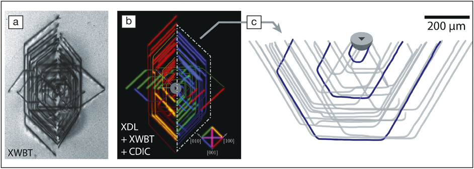
First, defects in the crystal are imaged with x-ray diffraction laminography (XDL). This technique uses x-ray diffraction to create two-dimensional (2D) projections of the defects at different viewing angles, which are then reconstructed into a three-dimensional (3D) image highlighting the spatial arrangements of the defects.
The defects are subsequently imaged with conventional x-ray white beam topography (XWBT). This technique produces 2D images that contain information on the Burgers vector associated with a dislocation, the vector describing the magnitude and direction of the resulting lattice distortion. In order to reliably identify individual dislocations in these images, the team used a simulation based on the XDL data to predict the location and appearance of defects in the XWBT images. By overlaying the simulated data on the XWBT images, the Burgers vector could be determined for individual dislocations.

a) Conventional 2D x-ray white beam topography (XWBT) image of a dislocation arrangement; (b) top view of the 3D picture obtained using the novel correlative approach, with the Burgers vectors color-coded; and (c) isolated view of a slip-band that enabled the researchers to identify the activity of a regenerative source of dislocations, noted in blue. XDL is x-ray diffraction laminography and CDIC is (circularly polarized) visible light differential interference contrast (CDIC) microscopy. Credit: D. Hänschke, KIT.
The final imaging technique, visible light differential interference contrast (DIC) microscopy, is useful for visualizing height differences at a crystal surface. The researchers found that by correlating DIC images of surface steps associated with the movement of dislocations to the internal 3D dislocation paths obtained from XDL images, individual dislocations could be linked to their impact on the surface.
One of the most attractive features of the approach is its comprehensiveness, according to Hänschke. “Information of different qualities is connected to one large picture: three-dimensional paths of the dislocations, the direction of deformation each defect carries (the Burgers vector), and how the dislocations inside the crystal are related, for example, to damage at the surface,” he says.
For Hänschke and his colleagues, this approach had an immediate practical application. They used it to study the formation of so-called slip-bands in silicon wafers, which are related to the plastic deformation that occurs during thermal processing. For this application, the team induced typical damage into a 20 × 20 mm2 piece of a wafer. Then, using their new approach, they imaged and characterized the network of 60 interconnected dislocations that emerged around the damaged area.
From the results, the research team determined the 3D dislocation paths with high spatial resolution, identified 98% of the orientations of the Burgers vectors, and linked 95% of the dislocations to surface features on the crystal. More generally, they related their observations to theoretical predictions of the driving forces behind slip-band formation and concluded that the mobilization and multiplication of preexisting dislocations dominate slip-band formation during thermal processing.
Matthew Horton, a researcher at Lawrence Berkeley National Laboratory with expertise in semiconductor dislocations, calls this approach “an important step in the right direction.” Studies of dislocations have led to many interesting, surprising, and important discoveries, he says, but the lack of tools has hindered progress.
“There are some excellent tools we have already, but they only give us a narrow window to look at dislocations. Therefore, any new tool, such as the one introduced by Hänschke and colleagues, is great news, both because it directly addresses a need in the community, and also because it will hopefully encourage more people to study dislocations,” Horton says.
Co-author Elias Hamann, also from KIT, agrees. “There are probably many interesting scientific questions out there that may now be answered, or at least be considered, from this completely new point of view.”


