Introduction
Electromagnetic interference (EMI) effects can decrease the signal-to-noise ratio and deteriorate reliability performances of electronic circuits and systems [Reference Pozar1]. The time-invariant EMI signals with already known frequencies and bandwidths can be suppressed by using the fixed filters [Reference Zhang and Wu2–Reference Lin and Wu9]. Generally, the EMI signals are variable with time and thus the reconfigurable filters are needed and have been widely researched [Reference Ma, Wang, Li and Chen10–Reference Ebrahimi, Baum, Scott and Ghorbani27]. The evanescent-mode cavity resonators with high unloaded quality factors have been applied to design reconfigurable bandstop filters (BSFs) with constant bandwidth in paper [Reference Hickle and Peroulis13]. The evanescent-mode cavity resonator has a multilayer structure which can increase the complexity and cost of fabrication and assembly. In paper [Reference Liu, Yang and Chi14], a lumped-element three-channel reconfigurable filter bank with wide frequency tuning range is presented. However, the size is relatively large by using three stand-alone reconfigurable filters. In paper [Reference Li and Yang19], the coupling microstrip resonators loaded by varactor diodes are applied to design a reconfigurable BSF with the frequency tuning range of 5.31–9.12 GHz (52.8%). In paper [Reference Zhang, Chan, Xue and Hu24], tunable resonators based on the doublet configuration are applied to design a reconfigurable BSF with the frequency tuning range of 1.73–2.2 GHz (23.9%). In paper [Reference Li, Chen, Chi and Yang26], tunable microstrip resonators with capacitive terminals are applied to design a reconfigurable BSF with the frequency tuning range of 11.3–16.5 GHz (37%). The microstrip defected ground structure resonators loaded by varactor diodes have been applied to design reconfigurable BSFs which have large radiation losses [Reference Ebrahimi, Baum, Scott and Ghorbani27]. For presented reconfigurable BSFs, the reconfigurable bandstop functions have been realized but the frequency tuning ranges are narrow and the designs of independent wide bandwidth tuning are rarely presented.
Generally, reconfigurable filters have reflective stopbands. However, the reflected electromagnetic power can deteriorate the dynamic range and create unwanted oscillations. To solve this problem, reconfigurable filters with absorptive stopbands have been presented [Reference Psychogiou and Gómez-García28–Reference Hickle and Peroulis32]. In paper [Reference Psychogiou and Gómez-García28], a tunable absorptive BSF with the frequency tuning range of 186–292 MHz (44%) and the stopband return loss larger than 10 dB has been presented. In paper [Reference Adhikari, Yang, Wu and Peroulis29], a tunable absorptive BSF with the frequency tuning range of 22.45–42.39 GHz (61.5%) and the stopband return loss larger than 5 dB has been presented. In paper [Reference Hickle and Peroulis32], four tunable absorptive BSFs with the same frequency tuning ranges of 1.0–2.3 GHz (78.8%) have been presented. As the quality factor values of the applied varactors are very small at lower stopband, the minimum stopband suppression can be obtained at the minimum stopband frequency and then the stopband suppression levels of the four tunable BSFs in paper [Reference Hickle and Peroulis32] are 5, 8, 5, and 10 dB, respectively. For the presented absorptive reconfigurable BSFs, the frequency and bandwidth tuning ranges are small and the stopband absorption ratio is insufficient under tuning processes. Furthermore, the extra stopband absorption circuits lead to large sizes, limits of frequency and bandwidth tuning ranges, and complicated tuning processes.
In this paper, an absorptive reconfigurable BSF with compact size and ultra-wide frequency tuning range using distributed lossy resonators is proposed. In each reconfigurable bandstop resonator, a varactor and a PIN diode are utilized as control and absorption devices. When the PIN diodes are in off and on states, the upper and lower frequency tuning ranges of stopbands can be obtained, respectively, to realize ultra-wide stopband frequency tuning range. Meanwhile, the stopband frequency and bandwidth tuning can be independently controlled by bias voltages. The resistances in the varactors and PIN diodes can dissipate the electromagnetic power and thus result in absorptive stopband without using extra stopband absorption circuits. Therefore, ultra-wide frequency tuning range and absorptive stopband can be obtained simultaneously. The stopband suppression level and stopband absorption ratio are proportional to the number of applied distributed lossy bandstop resonators. Small passband insertion loss and high stopband absorption ratio can be realized simultaneously.
The remainder is organized as follows. Firstly, the design and analysis of absorptive reconfigurable BSF are presented. Then, the absorptive reconfigurable BSFs using a pair of distributed lossy resonators and multiple pairs of distributed lossy resonators are presented, respectively. Afterward, the experiment results of the absorptive reconfigurable BSF with six pairs of distributed lossy resonators are presented. Finally, brief conclusions are given.
Design and analysis of absorptive reconfigurable BSF
Generally, reconfigurable BSFs have reflective stopbands. To realize absorptive reconfigurable BSFs, the conventional approach is to add extra stopband absorption circuits. Figure 1(a) shows a schematic of absorptive reconfigurable BSFs with extra stopband absorption circuits. Figure 1(b) shows that two reconfigurable bandpass filters (BPFs) and two absorption resistors have been applied to design the stopband absorption circuits in absorptive reconfigurable BSFs. The resistance value Z 0 is equivalent to the characteristic impedance of the port, which is usually 50 Ω. Moreover, the center frequencies f 1 = f 2 = f 3 and the bandwidths BW1 = BW2 = BW3 should be satisfied. However, there are four major issues exist in the absorptive reconfigurable BSFs with extra reconfigurable stopband absorption circuits.
(1) The frequency tuning ranges of the reconfigurable BPFs turn out to be a limitation to the frequency tuning range of the absorptive reconfigurable BSF.
(2) The bandwidth tuning ranges of the reconfigurable BPFs turn out to be a limitation to the bandwidth tuning range of the absorptive reconfigurable BSF.
(3) The frequencies and bandwidths of the reconfigurable BSF and reconfigurable BPFs need to be the same which can lead to very complicated tuning processes.
(4) The additional stopband absorption circuits can increase the total dimension to a large extent.

Figure 1. Schematic of absorptive reconfigurable BSFs with stopband absorption circuits. (a) Complete schematic. (b) Stopband absorption circuits.
To solve the above issues of absorptive reconfigurable BSFs with extra stopband absorption circuits, an absorptive reconfigurable BSF with compact size and ultra-wide frequency tuning range using distributed lossy resonators is proposed for the first time. The design and analysis processes are given as follows.
Absorptive reconfigurable BSF using a pair of distributed lossy resonators
Figure 2(a) shows a schematic of the absorptive reconfigurable BSF using a pair of distributed lossy resonators which are symmetrically located at both sides of the microstrip line. The input and output microstrip line has the characteristic impedance of 50 Ω. Each lossy bandstop resonator consists of a capacitor, a varactor diode, a PIN diode, and two sets of voltage bias circuits. The PIN diode is connected to a short-circuit microstrip line which can adjust the frequency tuning range at the on state of the PIN diode. The equivalent circuit of a varactor diode is given in Fig. 2(b). It should be noted that the series resistor Rs, series inductor Ls, and packaging capacitor Cp have fixed values, while the values of junction resistor Rj and junction capacitor Cj can be changed by the bias voltage. The equivalent circuits of a PIN diode in on and off states are given in Fig. 2(c) and (d), respectively. Based on the Joule’s law, the power dissipated by the resistor R can be expressed as
 \begin{equation}{P_{loss}}\left( R \right) = \frac{1}{2}{\left| {I\left( R \right)} \right|^2}R = \frac{1}{2}\frac{{{{\left| {V\left( R \right)} \right|}^2}}}{R}.\end{equation}
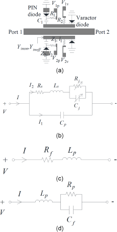
Figure 2. (a) Schematic of absorptive reconfigurable BSF using a pair of resonators. (b) Equivalent circuit of varactor diode. (c) Equivalent circuit of PIN diode in on state. (d) Equivalent circuit of PIN diode in off state.
The equivalent circuits of the proposed lossy bandstop resonator at on and off states of the PIN diode are shown in Fig. 3(a) and (b), respectively. When the PIN diode is in on state, the input admittance Yinon of the lossy bandstop resonator can be derived as follows:
 \begin{equation}{Y_{in1}} = \frac{{{Z_1} + j{Z_v}\tan {\beta _1}{l_1}}}{{{Z_1}{Z_v} + jZ_1^2\tan {\beta _1}{l_1}}}\end{equation}
 \begin{equation}{Z_v} = \frac{{{Z_{v1}}}}{{1 + j\omega {Z_{v1}}{C_p}}}\end{equation}
 \begin{equation}{Z_{v1}} = {R_s} + j\omega {L_s} + \frac{{{R_j}}}{{1 + j\omega {R_j}{C_j}}}\end{equation}
 \begin{equation}{Y_{in2}} = \frac{1}{{\frac{1}{{j\omega {C_1}}} + {R_f} + j\omega {L_p} + j{Z_2}\tan {\beta _2}{l_2}}}.\end{equation}
Figure 3. Equivalent circuits of the proposed bandstop resonator. (a) On state. (b) Off state.
When the PIN diode is in off state, the input admittance Yinoff of the lossy bandstop resonator can be derived as follows:
 \begin{equation}{Y_{in3}} = \frac{1}{{\frac{1}{{j\omega {C_1}}} + j\omega {L_p} + \frac{{{R_p}}}{{1 + j\omega {R_p}{C_f}}} + j{Z_2}\tan {\beta _2}{l_2}}}.\end{equation}
Hence, the stopband resonant frequency at the on state of the PIN diode can be expressed as
while the stopband resonant frequency at the off state of the PIN diode can be expressed as
 \begin{equation}\operatorname{Im} \left[ {{Y_{inoff}}} \right] = 0.\end{equation}
The resistances in the varactors and PIN diodes can dissipate the electromagnetic power at stopband resonant frequencies and result in absorptive stopband without using extra absorptive circuits. To investigate the stopband absorption performance, the simulated frequency responses of the absorptive reconfigurable BSF using a pair of distributed lossy resonators at Cj of 0.55 pF and off state of the PIN diodes are shown in Fig. 4. It shows that the S 11 = −8.329 dB, S 21 = −4.476 dB at the frequency of 5 GHz. The equation to calculate the stopband absorption ratio is given as follows:
 \begin{equation}\left( {1 - {{\left| {{S_{11}}} \right|}^2} - {{\left| {{S_{21}}} \right|}^2}} \right) \times 100\%. \end{equation}
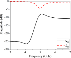
Figure 4. Frequency responses of the absorptive reconfigurable BSF using a pair of resonators at Cj of 0.55 pF and off state of PIN diodes.
Therefore, the calculated stopband absorption ratio is 49.6%. To increase the stopband suppression level and stopband absorption ratio, the absorptive reconfigurable BSF using multiple pairs of distributed lossy resonators can be applied and design procedures are given as follows.
Absorptive reconfigurable BSF using multiple pairs of distributed lossy resonators
Figure 5 shows a generalized schematic of the absorptive reconfigurable BSF with N distributed lossy resonators. The gap distance between adjacent resonators in the horizontal direction is 1.5 mm. The optimized value of C 1 is 3 pF.

Figure 5. Generalized schematic of absorptive reconfigurable BSF using N distributed lossy resonators.
To analyze relationships between the number of resonators, stopband suppression level, and stopband absorption ratio, the frequency responses of the absorptive reconfigurable BSFs with different numbers of resonators are simulated for comparison. At N of 10, 12, and 14 and Cj of 0.55 pF, the frequency responses of the absorptive reconfigurable BSFs at the on and off states of PIN diodes are shown in Fig. 6(a) and (b), respectively. At the on state of PIN diodes, the stopband suppression levels are −8.694, −10.477, and −11.911 dB for N of 10, 12, and 14, respectively. The stopband reflection coefficients are −13.976, −12.582, and −12.946 dB for N of 10, 12, and 14, respectively. Therefore, the stopband absorption ratios are 82.5%, 85.5%, and 88.5% for N of 10, 12, and 14, respectively. At the off state of PIN diodes, the stopband suppression levels are −25.81, −31.236, and −35.831 dB for N of 10, 12, and 14, respectively. The stopband reflection coefficients are −10.476, −10.421, and −10.52 dB for N of 10, 12, and 14, respectively. Therefore, the stopband absorption ratios are 90.7%, 90.8%, and 91.1% for N of 10, 12, and 14, respectively. Therefore, the stopband suppression level and stopband absorption ratio of the proposed absorptive reconfigurable BSF can be improved by increasing the number of distributed lossy resonators.
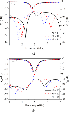
Figure 6. Frequency responses of the absorptive reconfigurable BSF at N of 10, 12, and 14 and Cj of 0.55 pF. (a) On state. (b) Off state.
Moreover, the stopband suppression level at the off state of PIN diodes is larger than the stopband suppression level at the on state of PIN diodes. The stopband return loss at the off state of PIN diodes is less than the stopband return loss at the on state of PIN diodes. The reason is that the distributed lossy resonator has a larger quality factor in off state than in on state of PIN diodes. As a result, the stopband suppression level and stopband absorption ratio are proportional to the number of applied distributed lossy resonators. However, the size of absorptive reconfigurable BSF is also proportional to the number of applied distributed lossy resonators.
To make a tradeoff between the stopband suppression level, stopband absorption ratio performances, and the total size, six pairs of distributed lossy resonators are applied to design the proposed absorptive reconfigurable BSF on the Taconic TLY-5 substrate with thickness of 0.508 mm and εr = 2.2. The geometrical dimensions are: L 1 = 7, L 2 = 1, W 0 = 1.54, W 1 = 0.5, W 2 = 1.2, and g 1 = 0.1, all in mm. The Skyworks SMP1320 PIN diodes and MACOM MA46H201 varactor diodes are applied to design the absorptive reconfigurable BSF. Table 1 gives the parameter values of the applied PIN diodes in both on and off states. For the applied varactor diodes, the fixed parameter values of Rs, Ls, and Cp are 0.5 Ω, 0.9 nH, and 0.15 pF, respectively. Figure 7 shows the variable parameters Cj and Rj of the applied varactor diode varying with the bias voltages which have the range of 0–25 V. Figure 8 shows a design flowchart of the proposed absorptive reconfigurable BSF. Detailed design procedures of the proposed absorptive reconfigurable BSF are given as follows.
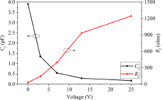
Figure 7. Cj and Rj varying with bias voltages.
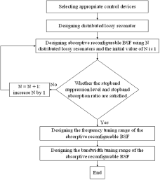
Figure 8. Design flowchart of the proposed absorptive reconfigurable BSF using distributed lossy resonators.
Table 1. Values of PIN diodes

The first step is to design the stopband frequency tuning of the absorptive reconfigurable BSF. The stopband frequency can be adjusted by the microstrip line with length L 1. Figure 9(a) shows the stopband frequencies varying with the length L 1 at the off state of PIN diodes and Cj of 0.29 pF using six pairs of distributed lossy resonators. When the length L 1 is increased, the stopband frequency is reduced. As a result, the length L 1 can be applied to determine the center frequency of the stopband frequency tuning range at the off state of PIN diodes. The short-circuit microstrip line with the length L 2 can adjust the frequency tuning range at the on state of PIN diodes. When the PIN diodes are in off and on states, the upper and lower frequency tuning ranges of stopband can be obtained, respectively. Therefore, the total stopband frequency tuning range which is the combination of the upper and lower frequency tuning ranges can be enhanced to a large extent and thus the ultra-wide stopband frequency tuning range of the proposed absorptive reconfigurable BSF can be realized.
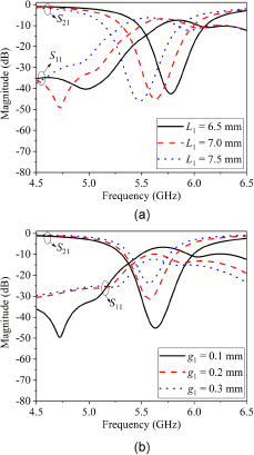
Figure 9. (a) Stopband frequency varying with L 1. (b) Stopband bandwidth varying with g 1.
The second step is to design the stopband bandwidth tuning of the proposed absorptive reconfigurable BSF. The stopband bandwidth can be adjusted by the gap g 1 which can adjust the coupling strength between the 50 Ω microstrip line and the distributed lossy resonator. Figure 9(b) shows the stopband bandwidths varying with the gap g 1 at the off state of PIN diodes and Cj of 0.29 pF using six pairs of distributed lossy resonators. When the gap g 1 is increased, the stopband bandwidth is reduced. To tune stopband bandwidth, resonators are divided into two groups, namely, resonators 1–6 for the first group and resonators 7–12 for the second group. Then, each group is provided by an independent bias voltage. When the two bias voltages have different values, two different resonant frequencies can be obtained to realize the stopband bandwidth tuning. It should be noted that the stopband suppression level is inversely proportional to the stopband bandwidth. Therefore, a tradeoff between the stopband suppression level and stopband bandwidth should be made.
The stopband frequency and bandwidth of the proposed absorptive reconfigurable BSF can be independently controlled by bias voltages. The resistances in the varactors and the PIN diodes can dissipate the electromagnetic power and result in absorptive stopband without using extra absorptive circuits. It should be noted that the electromagnetic power absorption exists at the stopband resonant frequencies of the distributed lossy resonators. Therefore, the small insertion losses in the passband of the proposed absorptive reconfigurable BSF can be well maintained.
Experiment results
Figure 10 shows a photograph of the fabricated absorptive reconfigurable BSF using six pairs of distributed lossy resonators. The Keysight ADS and Ansys HFSS simulators are used herein for simulations, while a vector network analyzer is applied in the measurements.

Figure 10. Photograph of fabricated absorptive reconfigurable BSF using six pairs of distributed lossy resonators.
Figure 11(a) shows the stopband frequency tuning at the off state of PIN diodes. The simulated upper frequency tuning range is 3.61–6.34 GHz (55%) with the stopband suppression level of 25 dB, while the measured upper frequency tuning range is 3.6–6.39 GHz (56%) with the stopband suppression level of 25 dB. Figure 11(b) shows the stopband frequency tuning at the on state of PIN diodes. The reduced stopband suppression level at the on state of PIN diodes is due to the reduced quality factor of bandstop resonators. The simulated lower frequency tuning range is 2.04–3.76 GHz (59%) with the stopband suppression level of 10 dB, while the simulated lower frequency tuning range with the stopband suppression level of 20 dB is 3.03–3.66 GHz (19%). The measured lower frequency tuning range is 2.04–3.76 GHz (59%) with the stopband suppression level of 10 dB, while the measured lower frequency tuning range with the stopband suppression level of 20 dB is 3.03–3.66 GHz (19%). Therefore, the measured total frequency tuning range is 3.03–6.39 GHz (71%) with the stopband suppression level of 20 dB, while the total measured frequency tuning range with the stopband suppression level of 10 dB is 2.04–6.39 GHz (103%). Moreover, the simulated and measured typical insertion losses in the passband are 0.5 dB and 1 dB, respectively.
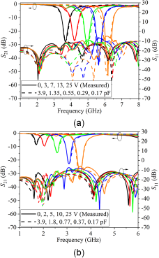
Figure 11. (a) Frequency tuning at off state of PIN diodes. (b) Frequency tuning at on state of PIN diodes.
At the off state of PIN diodes, the simulated minimum stopband return losses at Cj of 3.9, 1.35, 0.55, 0.29, and 0.17 pF are 10.6, 11.1, 9.8, 6.6, and 5.3 dB, respectively. Meanwhile, the simulated stopband suppression level at Cj of 3.9, 1.35, 0.55, 0.29, and 0.17 pF are 27.7, 27.2, 31.2, 45.1, and 53.2 dB, respectively. The measured minimum stopband return losses at bias voltages of 0, 3, 7, 13, and 25 V are 11.6, 11, 8.8, 6.5, and 5 dB, respectively. The measured stopband suppression level at bias voltages of 0, 3, 7, 13, and 25 V are 27.7, 27.2, 31.2, 45.2, and 53.2 dB, respectively. At the on state of PIN diodes, the simulated minimum stopband return losses at Cj of 3.9, 1.8, 0.77, 0.37, and 0.17 pF are 12.1, 13.2, 10.7, 8.2, and 6 dB, respectively. Meanwhile, the simulated stopband suppression level at Cj of 3.9, 1.8, 0.77, 0.37, and 0.17 pF are 8.5, 10, 14.5, 22.8, and 34.9 dB, respectively. The measured minimum stopband return losses at bias voltages of 0, 2, 5, 10, and 25 V are 13, 15, 11.3, 7.5, and 6.2 dB, respectively. The measured stopband suppression level at bias voltages of 0, 2, 5, 10, and 25 V are 8.5, 10, 14.5, 22.8, and 34.5 dB, respectively.
Figure 12(a) shows the stopband absorption ratio of the absorptive reconfigurable BSF at the off state of PIN diodes. It shows that the simulated stopband absorption ratio is larger than 70%, while the measured stopband absorption ratio is larger than 68%. Figure 12(b) shows the stopband absorption ratio of the absorptive reconfigurable BSF at the on state of PIN diodes. It shows that the simulated stopband absorption ratio is larger than 75%, while the measured stopband absorption ratio is larger than 76%.
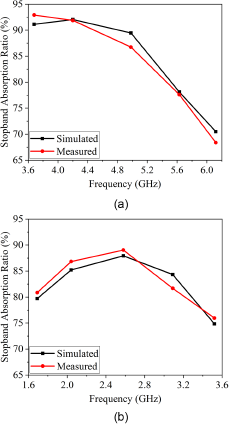
Figure 12. (a) Stopband absorption ratio at off state of PIN diodes. (b) Stopband absorption ratio at on state of PIN diodes.
Figure 13 shows the measured stopband bandwidth tuning of the absorptive reconfigurable BSF at the off state of PIN diodes with the bias voltage V 1 to varactors 1–6 at 8 V and the other bias voltage V 2 to varactors 7–12 at 8, 10, and 12 V, respectively. It shows that the stopband bandwidth tuning range is 510–820 MHz at the 10 dB stopband suppression level. Moreover, at the 10 dB stopband suppression level, the stopband frequency ranges are 4.87–5.38 GHz, 4.96–5.59 GHz, and 4.99–5.81 GHz at V 2 of 8 V, 10 V, and 12 V, respectively. The stopband absorption ratios at 10 dB stopband suppression level are larger than 80%, 84%, and 81% at V 2 of 8 V, 10 V, and 12 V, respectively. Therefore, the proposed absorptive reconfigurable BSF can maintain high stopband absorption ratio when the stopband bandwidth is tuned.
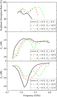
Figure 13. Bandwidth tuning of absorptive reconfigurable BSF.
The total dimension of the absorptive reconfigurable BSF is 49.5 mm × 10.34 mm, which is equivalent to 0.46 λg × 0.1 λg, where λg is the guided wavelength of 50 Ω microstrip line at 2.04 GHz. Table 2 lists comparisons with other reconfigurable BSFs. It can be observed that this work has achieved compact size, ultra-wide stopband frequency tuning range, absorptive stopband, and independent stopband bandwidth tuning.
Table 2. Comparisons with other reconfigurable BSFs

Conclusion
An absorptive reconfigurable BSF with compact size and ultra-wide frequency tuning range using distributed lossy resonators has been presented. In each reconfigurable lossy bandstop resonator, a varactor and a PIN diode are utilized as the control and absorption devices. When the PIN diodes are in off and on states, the upper and lower frequency tuning ranges of stopbands can be obtained, respectively, to realize ultra-wide stopband frequency tuning range. The measured total frequency tuning range is 3.03–6.39 GHz (71%) with the stopband suppression level of 20 dB, while the measured total frequency tuning range with the stopband suppression level of 10 dB is 2.04–6.39 GHz (103%). The resistances in the varactors and PIN diodes can dissipate the electromagnetic power and thus result in absorptive stopband without using extra absorptive circuits. The presented absorptive reconfigurable BSF has achieved compact size, ultra-wide frequency tuning range, absorptive stopband, and independent stopband bandwidth tuning and thus can be applied to mitigate EMI effects in electronic circuits and systems.
Acknowledgements
This work was supported by the Guangdong Basic and Applied Basic Research Foundation under grant number 2021A1515110454.
Competing interests
The author reports no conflict of interest.

Qun Li received the B.S. degree from Southwest Petroleum University, Chengdu, China, in 2012, and the Ph.D. degree from the University of Electronic Science and Technology of China (UESTC), Chengdu, in 2018.
In 2017, he joined the Department of Electrical and Computer Engineering, Wayne State University, Detroit, MI, USA, as a Research Scholar. From 2017 to 2018, he was a Research Scholar with the Department of Electrical and Computer Engineering, Rutgers University, New Brunswick, NJ, USA. From 2018 to 2020, he was a Post-Doctoral Researcher with UESTC. From 2020 to 2023, he was a Post-Doctoral Researcher with Sun Yat-sen University, Guangzhou, China. From 2021 to 2022, he was a Visiting Fellow with City University of Hong Kong, Hong Kong. He is currently a Post-Doctoral Fellow with the Hong Kong University of Science and Technology, Hong Kong. His current research interests include electromagnetics, antennas, circuits, and systems.


